Image Generated Using DALL·E
The Yield Economic Of Semiconductor Manufacturing
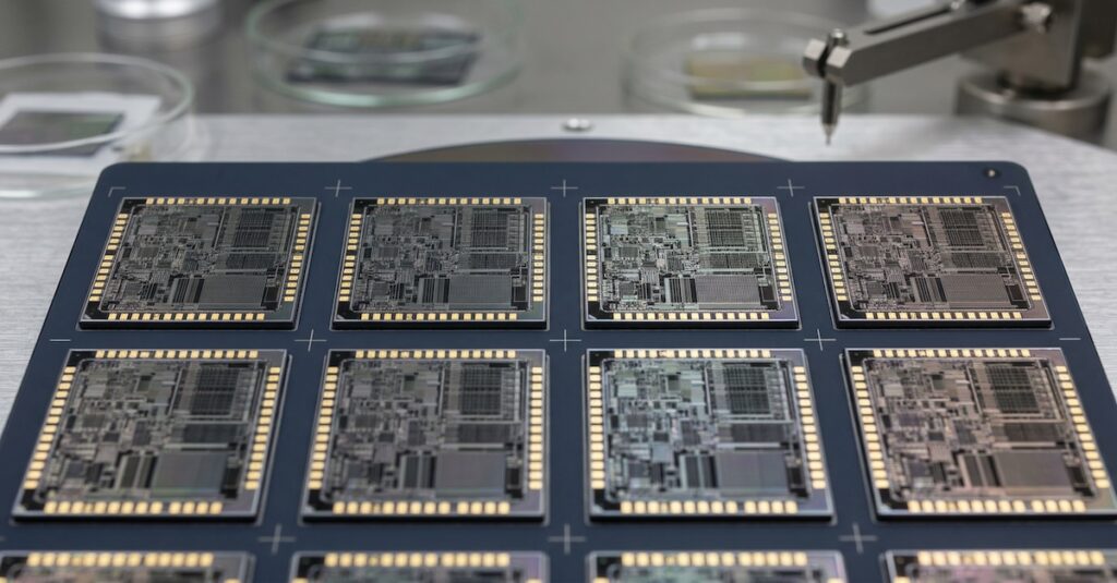
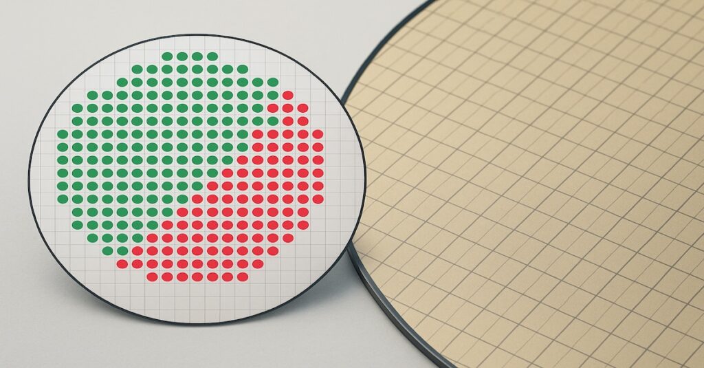
Yield is the percentage of functional chips produced per wafer and is the foundation of semiconductor economics. Every wafer starts as a costly investment in materials, equipment time, and process precision.
When more dies on that wafer, work perfectly, and each functional chip costs less to produce, margins and profitability improve directly.
At advanced technology nodes, where wafer costs can exceed tens of thousands of dollars, even a 1% yield gain can translate into millions in savings. This is why yield is not just a technical metric. It is a financial one. High yield lowers cost per die, improves gross margin, and enables companies to price products more competitively.
As process complexity grows, yield becomes harder to maintain. Each new node introduces tighter tolerances and new failure modes, linking technical precision and financial outcome more closely than ever.
In essence, yield is the quiet bridge between engineering excellence and economic success and the factor that decides whether innovation becomes profit.
How Data-Driven Yield Management System Have Evolved
Yield management has advanced from manual inspection to intelligent, data-driven automation, a transformation shaped by decades of progress in data collection, analytics, and system integration. As semiconductor processes grew more complex, traditional visual checks and spreadsheets could no longer keep pace with the precision required to sustain competitive yields.
Modern fabs now deploy Yield Management Systems (YMS) that integrate real-time data, advanced analytics, and machine learning to transform yield from a passive metric into a predictive, actionable insight. The table below outlines this evolution:
| Era | Key Characteristics | Data Capabilities | Challenges |
|---|---|---|---|
| Manual Era (1980s–2000s) | Visual inspections, manual SPC charts, and basic defect tracking. | Limited data collection and offline analysis using spreadsheets. | Slow feedback loops, poor traceability, reactive response. |
| Advanced Era (2000s–2020s) | Automated SPC, digital defect logging, and integrated tool monitoring. | Centralized data storage with faster trend analysis and limited automation. | Limited predictive analytics, partial integration across systems. |
| Automated Era (2020s–Present) | Real-time data acquisition from MES, metrology, and sensors. | Full integration with cloud computing, AI/ML-based yield prediction, and cross-fab traceability. | Managing large data volumes, ensuring interpretability of AI results. |
In the early decades, engineers tracked yield using simple control charts and manual logs. These methods provided limited visibility and slow feedback, often revealing problems only after yield had already been lost.
As wafer complexity increased, manual processes could no longer scale. Semiconductor manufacturers began integrating automated data collection and Statistical Process Control (SPC) into production lines, enabling faster detection of process drifts and systematic analysis of defect trends. This marked the transition from reactive monitoring to structured yield control, where data became central to manufacturing stability.
| Feature | Description | Purpose And Impact |
|---|---|---|
| Data Acquisition Layer | Real time interface with MES, metrology, and inspection tools | Enables continuous monitoring and instant process feedback |
| Statistical Process Control (SPC) | Automated Cp Cpk tracking, control charts, and deviation alerts | Ensures process stability and early defect detection |
| Fault Detection and Classification (FDC) | Algorithms identify and categorize process or tool abnormalities | Prevents downtime by enabling predictive maintenance |
| Machine Learning Analytics | Uses PCA, random forests, and anomaly detection for yield prediction | Detects subtle variations that impact yield before failure occurs |
| Visualization Dashboards | Unified display of yield, WAT, and test data across tools and lots | Improves decision speed and cross functional collaboration |
Today, modern fabs operate within a fully connected analytics ecosystem. Yield Management Systems now merge real-time data acquisition, advanced visualization, and machine learning to predict yield excursions before they occur.
These systems link data from metrology, inline inspection, test, and equipment health monitoring into a unified view, empowering engineers to act proactively rather than retroactively. This evolution has redefined yield from a diagnostic indicator into a strategic, data-driven performance metric.
Cost, ROI, And The Business Of Yield
Deploying a Yield Management System involves both technical and financial commitments. Semiconductor manufacturing involves substantial capital costs, including tools, cleanrooms, and data infrastructure.
Implementing a YMS adds software licensing, integration, and personnel training expenses, but it also transforms how that investment performs.
By reducing variability, minimizing scrap, and accelerating problem resolution, yield improvements translate directly into lower cost per die and more substantial gross margins. Even a slight percentage increase in yield at advanced nodes can generate multi-million-dollar savings across high-volume production.
The return on investment extends beyond immediate cost reduction. Higher yields shorten time-to-market, improve equipment utilization, and stabilize supply. These gains compound over a product’s lifecycle, improving financial predictability and enabling greater reinvestment in research and development.
In essence, a well-implemented Yield Management System becomes not only a quality tool but a profit multiplier, turning data intelligence into sustained economic advantage.
The Transition From Automation To Intelligence
Semiconductor yield management is entering a new phase where automation alone is no longer enough. The focus is shifting toward systems that think, learn, and respond in real time. Yield Management Systems are evolving to integrate machine learning, hybrid cloud data platforms, and inline process feedback.
These advancements allow fabs to identify deviations earlier, make predictive corrections, and maintain consistent output even as manufacturing complexity continues to rise.
The future of yield management lies in intelligence that is both adaptive and interpretable. Systems will not only detect issues but also understand why they occur and recommend precise corrective actions. This transformation will redefine yield as a measure of insight rather than output.
In this intelligent era, yield becomes a continuous learning loop, linking every wafer, process, and decision into a unified path of improvement and resilience.