Image Generated Using DALL·E
From Node-Centric To Workload-Centric
For more than five decades, semiconductor innovation revolved around a single pursuit: shrinking transistors. Each new process node promised higher density, lower cost per function, and faster circuits. This node-centric model powered the industry through its golden era, making smaller equivalent to better. As the limits of atomic scale physics approach, that once predictable equation no longer holds.
Progress is now measured by workload alignment rather than by node advancement.
The key question for designers is not how small the transistors are but how well the silicon reflects the behavior of the workload it runs. This marks a fundamental transformation from process-driven evolution to purpose-driven design.
To understand how this transformation unfolds, it is essential to define what workload awareness means and why it changes the way semiconductors are built.
The Concept Of Workload Awareness
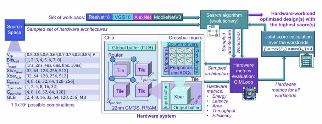
Workload awareness begins with the recognition that computation is not uniform. Each class of workload, such as neural network training, radar signal analysis, or camera data processing, shows distinct patterns of data flow, temporal locality, and parallelism. Recognizing these patterns allows designers to shape architectures that match computation to structure instead of forcing different workloads through one standard design.
Traditional architectures focused on generic performance through higher frequency, larger caches, or more cores. Such approaches often waste energy when the actual bottleneck lies in memory bandwidth, communication latency, or synchronization overhead. A workload-aware design begins with profiling. It identifies how data moves, where stalls occur, and how operations scale in time and energy.
| Workload Type | Key Characteristics | Architectural Focus | Example Design Responses |
|---|---|---|---|
| AI Training | Dense linear algebra, large data reuse, high bandwidth demand | Compute density and memory throughput | Tensor cores, high bandwidth memory, tiled dataflow |
| AI Inference (Edge) | Low latency, sparsity, temporal reuse | Energy efficient compute and memory locality | On chip SRAM, pruning aware accelerators |
| Automotive | Real time, deterministic, mixed signal | Low latency interconnect, redundancy | Lockstep cores, time sensitive networks |
| Signal Processing | Streaming data, predictable compute patterns | Deterministic pipelines, throughput balance | DSP arrays, low latency buffers |
| Industrial Control | Small data sets, long lifetime, low cost | Reliability and integration | Mature nodes, embedded NVM |
This awareness reshapes design philosophy. Instead of optimizing transistors alone, engineers now optimize data pathways, compute clusters, and memory placement based on the workload characteristics.
In practical terms, this means choosing architectural topologies such as mesh fabrics, matrix engines, or local scratchpads that mirror the natural behavior of the workload.
The Architectural Shifts
The move from node-centric to workload-centric design is transforming semiconductor architecture. Efficiency now depends on how well compute, memory, and packaging align with the behavior of each workload rather than how advanced the process node is.
This transformation spans the entire hierarchy. Every layer, from compute logic to system orchestration, must now reflect how data flows and where energy is spent.
Key Architectural Shifts
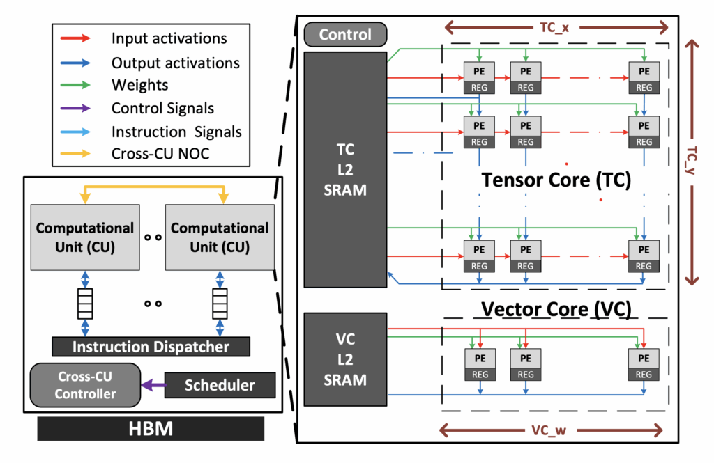
- Compute: Transition from monolithic processors to heterogeneous clusters with domain-specific accelerators such as matrix engines, DSPs, and control cores.
- Memory: Focus moves from capacity to proximity. Data is placed closer to the compute using high bandwidth memory, embedded DRAM, or stacked SRAM.
- Packaging: The package becomes an architectural canvas. Two-and-a-half-dimensional and three-dimensional integration combine logic, memory, and analog dies from multiple nodes.
- Interconnect: Movement from fixed buses to scalable low-latency fabrics using silicon bridges, interposers, and emerging optical links.
- System Orchestration: Compilers and runtime software allocate resources dynamically, adapting to workload behavior in real time.
These shifts mark a deeper alignment between physical design and computational intent. Each layer now collaborates to express the workload rather than merely execute it.
When compute, memory, and packaging act as a unified system, hardware becomes adaptive by design. This forms the core of the workload-aware architecture and sets the stage for a new scaling model driven by purpose instead of geometry.
Workload-Based Scaling Law
For many decades, semiconductor progress followed a simple path: smaller transistors meant faster, cheaper, and more efficient chips. That rule of geometric improvement, often described as Moore’s Law, guided every roadmap. As scaling reaches physical and economic limits, the performance gains once guaranteed by smaller nodes have diminished.
Today, most power is spent moving data rather than switching transistors, and actual efficiency depends on how well the architecture aligns with the workload itself.
Workload-based scaling redefines progress as performance per watt per workload. It evaluates how compute, memory, and interconnect cooperate to execute a specific data pattern with minimal energy. A well-tuned architecture at a mature node can outperform an advanced node if it matches the workload precisely.
This marks a transition from geometry to behavior, from transistor count to data awareness. Future leadership in semiconductors will belong to those who design not for smaller features, but for smarter alignment between computation and workload intent.