Image Generated Using Nano Banana
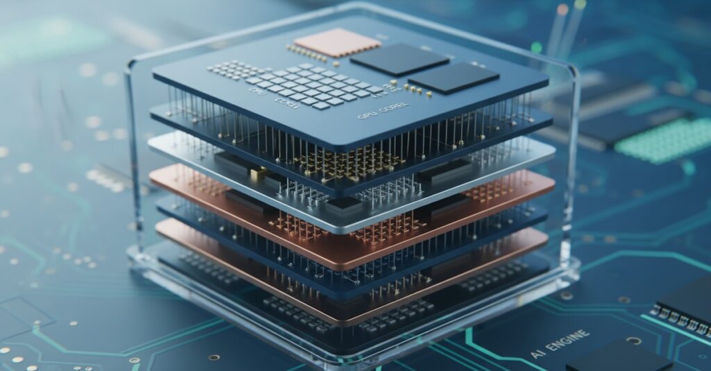
Semiconductor Simulator Landscape
Modern semiconductor innovation is no longer driven solely by physical experimentation. As device scaling, advanced packaging, and heterogeneous integration continue to increase complexity, simulation has become the invisible backbone of semiconductor development. Today’s chips are effectively born inside simulators long before silicon exists.
The semiconductor simulator landscape is not a single tool or category. Instead, it is a layered ecosystem of simulation environments operating across different physics domains, abstraction levels, and design objectives. From lithography and process modeling to device physics, compact model extraction, circuit verification, and system-level validation, each simulator plays a specific role in reducing uncertainty and accelerating decision-making.
The reason this layered structure exists is fundamentally architectural. Higher-fidelity physics simulations provide deeper insight but demand significant computational resources, while higher-level abstractions enable speed and scalability at the cost of physical detail. Together, they create a structured workflow where decisions evolve from physics to products.
Understanding this landscape is increasingly important as AI-driven digital twins, multi-physics coupling, and cloud-scale compute reshape semiconductor engineering.
Why Semiconductor Simulation Exists As A Stack
Semiconductor development spans multiple scales simultaneously.
At one end are atomic-level transport effects and quantum confinement; at the other are system-level performance and power efficiency. No single simulator can capture all these dimensions efficiently.
As a result, the industry relies on a hierarchy of simulators:
- Physics-intensive tools provide detailed insight into processes and device behavior.
- Compact models translate physical behavior into circuit-usable representations.
- Circuit simulators validate functionality and performance.
- Mixed-signal and system simulators evaluate integration and architecture.
- Reliability and multiphysics tools ensure long-term integrity under real operating conditions.
Each layer reduces complexity while preserving essential behavior from the layer below.
This flow allows engineering teams to move from process innovation to manufacturable products without relying solely on costly silicon iterations.
The Core Simulator Categories
Semiconductor simulation is best understood as a set of specialized simulator classes, each optimized for a different combination of physics fidelity, scale, and design-flow timing. No single simulator can answer every question efficiently, so teams rely on a layered landscape that moves from virtual fabrication and physics insight toward design verification, signoff, and system validation.
In practice, these categories work like a handoff pipeline. Process and lithography simulation shape the as-fabricated geometry. TCAD predicts device behavior. Compact models translate physics into PDK-ready abstractions. Circuit, mixed-signal, and system simulators validate functionality at scale. Reliability and multiphysics tools then close the loop by ensuring designs survive real-world stress across silicon, package, and system conditions.
| Simulator Category | Role |
|---|---|
| Lithography And Computational Lithography | Predict wafer printability and optimize masks and process windows for manufacturability |
| Process And Topography Simulation | Virtualize fabrication steps to create realistic device structures and material profiles |
| Device TCAD | Simulate electrical behavior using physics-based transport and electrostatic models |
| Quantum And Atomistic Device Simulation | Model quantum confinement and nanoscale transport in advanced or novel devices |
| Compact Model Extraction And Validation | Translate device physics into efficient PDK-ready models for circuit design |
| Circuit Simulation | Verify circuit functionality and performance using compact transistor models |
| Mixed-Signal Co-Simulation | Validate analog and digital interaction within integrated SoC environments |
| Behavioral And HDL Simulation | Verify digital logic functionality at high speed and large design scale |
| System-Level Simulation | Explore architecture-level performance, workloads, and system tradeoffs |
| Multiphysics And Reliability Signoff | Ensure electrical, thermal, mechanical, and aging integrity before production |
A useful way to select among these categories is to align the simulator with the engineering decision being made. Lithography simulation is used when evaluating printability and pattern fidelity. Process simulation and TCAD are used to assess device performance across process options. Compact models and SPICE-class solvers support circuit-level verification across corners and parasitics. Mixed-signal co-simulation is essential for validating full SoC behavior when the analog and digital domains interact.
Most modern teams also treat workflow orchestration as part of the simulator category itself, because value is created through repeatability, including parameter sweeps, calibration loops, model governance, and automated handoffs. This is also where AI-augmented calibration, surrogate models, and digital-twin strategies increasingly sit, wrapping multiple simulator layers to accelerate convergence from physics to product.
How Simulators Connect Across the Flow
The true strength of the semiconductor simulator landscape does not come from individual tools, but from how they connect across the development flow. Each simulator class produces information that becomes the foundation for the next layer of decision-making. Lithography and process simulation define manufacturable structures. Device-level physics transforms those structures into electrical behavior.
Compact models convert physics into scalable abstractions that power circuit design. Circuit and mixed-signal environments validate functionality, while system-level simulation ensures architectural goals are met. Finally, multiphysics and reliability analysis confirm that the design remains robust under real operating conditions.
This continuous handoff of models, data, and insights transforms simulation from isolated analysis into a coordinated engineering pipeline. As complexity increases across advanced nodes, heterogeneous integration, and multi-die systems, maintaining consistency across these layers becomes critical. Errors or misalignment introduced early in the flow can propagate downstream, increasing risk, cost, and iteration time.
Looking ahead, semiconductor simulation is moving toward tighter orchestration, with automation, AI-driven calibration, and digital twin frameworks linking multiple simulator layers into a unified decision engine. The future landscape will be defined less by individual simulators and more by how effectively organizations integrate them into repeatable, scalable workflows. In that environment, simulation is no longer just a validation step at the end of design. It becomes the continuous thread connecting physics, design intent, manufacturing reality, and long-term product performance.