Image Generated Using Nano Banana
Reliance Of AI And Data Workloads On Computer Architecture
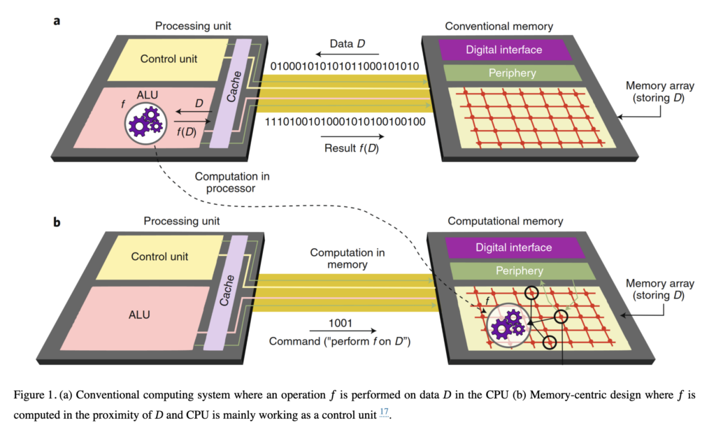
AI and modern data workloads have transformed how we think about computing systems. Traditional processors were designed for sequential tasks and moderate data movement. Today’s AI models work with enormous datasets and large numbers of parameters that must move constantly between memory and compute units. This movement introduces delays and consumes significant energy. As a result, memory bandwidth and the distance to the data have become major performance bottlenecks.
Graphics processors, tensor accelerators, and custom architectures try to address these issues by increasing parallelism. Yet, parallel computing alone cannot solve the challenge if data cannot reach the compute units fast enough. The cost of moving data inside a system is now often higher than the cost of the computation itself.
This places the spotlight on the relationship between compute location, memory hierarchy, and data flow. As models grow in size and applications demand faster responses, the gap between processor speed and memory access continues to widen.
The computing industry often refers to this as the memory wall. When AI tasks require moving gigabytes of data per operation, each additional millimeter of distance within a chip or package matters. To break this pattern, new approaches look at placing compute engines closer to where data is stored.
This shift has sparked interest in Processor In-Memory and Processing Near-Memory solutions.
Instead of pulling data along long paths, the system reorganizes itself so that computation occurs either within the memory arrays or very close to them. This architectural change aims to reduce latency, cut energy use, and support the growing scale of AI workloads.
What Is Processor-In-Memory And Processing-Near-Memory
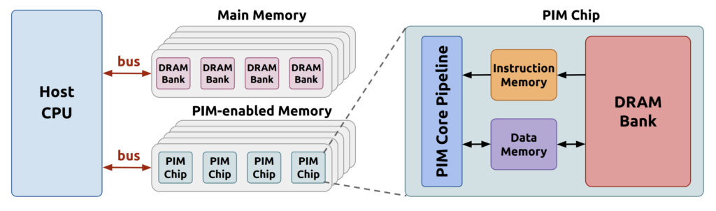
Processor-In-Memory places simple compute units directly inside memory arrays. The idea is to perform certain operations, such as multiplication and accumulation, inside the storage cells or peripheral logic. By doing this, data does not need to travel to a separate processor. This can lead to significant improvements in throughput and reductions in energy consumption for specific AI tasks, especially those involving matrix operations.
Processing-Near-Memory keeps memory arrays unchanged but integrates compute units very close to them, usually on the same stack or interposer. These compute units are not inside the memory but sit at a minimal distance from it. This enables faster data access than traditional architectures without requiring significant changes to memory cell structures. PNM often offers a more flexible design path because memory vendors do not need to modify core-array technology.
Here is a simple comparison of the two approaches.
| Feature | Processor-In-Memory | Processing-Near-Memory |
|---|---|---|
| Compute location | Inside memory arrays or peripheral logic | Adjacent to memory through same stack or substrate |
| Memory modification | Requires changes to memory cell or array design | Uses standard memory with added compute units nearby |
| Data movement | Very low due to in-array operation | Low because compute is positioned close to data |
| Flexibility | Limited to specific operations built into memory | Wider range of compute tasks possible |
| Technology maturity | Still emerging and specialized | More compatible with existing memory roadmaps |
Both approaches challenge the long-standing separation between computing and storage. Instead of treating memory as a passive container for data, they treat it as an active part of the computation pipeline. This helps systems scale with the rising demands of AI without relying entirely on larger, more power-hungry processors.
Research Efforts For Processor In Memory And Processing Near Memory
Research activity in this area has grown quickly as AI and data workloads demand new architectural ideas. Both Processor In Memory and Processing Near Memory have attracted intense attention from academic and industrial groups. PIM work often focuses on reducing data movement by performing arithmetic inside or at the edge of memory arrays. At the same time, PNM research explores programmable compute units placed near memory stacks to improve bandwidth and latency.
The selected examples below show how each direction is pushing the boundaries of energy efficiency, scalability, and workload suitability.
| Category | Example Work | Key Focus | What It Demonstrates | Link |
|---|---|---|---|---|
| Processor In Memory | SparseP: Efficient Sparse Matrix Vector Multiplication on Real PIM Systems (2022) | Implements SpMV on real PIM hardware | Shows strong gains for memory-bound workloads by computing inside memory arrays | Paper |
| Processor In Memory | Neural-PIM: Efficient PIM with Neural Approximation of Peripherals (2022) | Uses RRAM crossbars and approximation circuits | Shows how analog compute in memory can accelerate neural networks while cutting conversion overhead | Paper |
| Processing Near Memory | A Modern Primer on Processing In Memory (Conceptual framework) | Defines PIM vs PNM in stacked memory systems | Clarifies architectural boundaries and highlights PNM integration paths in 3D memory | Paper |
| Processing Near Memory | Analysis of Real Processing In Memory Hardware (2021) | Evaluates DRAM with adjacent compute cores | Provides methods used widely in PNM evaluation for bandwidth and workload behavior | Paper |
This comparison above captures both experimental implementations and architectural frameworks.
Together, they show how PIM pushes compute directly into memory structures, while PNM enables more flexible acceleration by placing logic close to high-bandwidth memory.
Implications And When Each Approach Can Benefit
Processor-In-Memory is often most useful when the workload is highly repetitive and dominated by simple arithmetic on large matrices. Examples include neural network inference and certain scientific operations. Since operations occur in memory, energy savings can be substantial. However, PIM is less suitable for general-purpose tasks that require flexible instruction sets or complex branching.
Processing-Near-Memory is a more adaptable option for systems that need performance improvements but cannot redesign memory cells. It supports tasks such as training large AI models, running recommendation engines, and accelerating analytics pipelines. Because PNM units are programmable, they can handle a broader range of workloads while still providing shorter data paths than traditional processors.
In real systems, both approaches may coexist. PIM might handle dense linear algebra while PNM handles control logic, preprocessing, and other mixed operations. The choice depends on workload structure, system integration limits, and power budgets. As AI becomes embedded in more devices, from data centers to edge sensors, these hybrids create new ways to deliver faster responses at lower energy.
The Direction Forward
The movement toward Processor-In-Memory and Processing-Near-Memory signals a larger architectural shift across the semiconductor world. Instead of treating compute and memory as separate units connected by wide interfaces, the industry is exploring tightly coupled designs that reflect the actual behavior of modern AI workloads. This shift helps push past the limits of conventional architectures and opens new opportunities for performance scaling.
As more applications rely on real-time analytics, foundation models, and data-intensive tasks, the pressure on memory systems will continue to increase. Designs that bring compute closer to data are becoming essential to maintaining progress. Whether through in-memory operations or near-memory acceleration, these ideas point toward a future where data movement becomes a manageable cost rather than a fundamental barrier.
The direction is clear. To support the next generation of AI and computing systems, the computing industry is rethinking distance, energy, and data flow at the chip level. Processor-In-Memory and Processing-Near-Memory represent two critical steps in that journey, reshaping how systems are built and how performance is achieved.