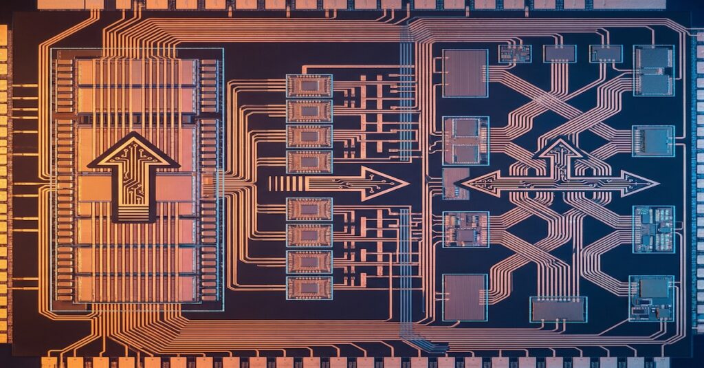
Image Generated Using Nano Banana
The Limits Of Silicon-Centric Thinking
For decades, semiconductor innovation was defined by silicon. Progress was driven by process node scaling, higher transistor density, and improvements in performance per watt. The industry followed a predictable roadmap anchored in lithography and device physics. Design, manufacturing, and test operated as separate stages, each focused on local optimization. Success was measured at the die level through yield, speed, leakage, and area.
This silicon focused approach is no longer sufficient. Scaling is slowing and the cost of advanced nodes continues to rise, reducing the impact of transistor level gains. At the same time, system requirements driven by AI, hyperscale infrastructure, and data intensive workloads are increasing in complexity. Performance is now shaped by how components interact across packaging, memory, interconnects, and software rather than by a single chip.
This creates a clear disconnect. Traditional semiconductor thinking optimizes the chip, while modern computing demands system level optimization. As a result, silicon alone can no longer meet application needs.
Closing this gap requires a shift from designing individual chips to engineering integrated systems where silicon operates as part of a broader architecture.
The Emergence Of System-Centric Semiconductor Engineering
The industry is shifting toward a system-centric model in which the boundaries between design, manufacturing, packaging, and deployment are increasingly blurred. Semiconductor engineering is no longer limited to RTL-to-GDSII flows. It now spans the full lifecycle from architecture definition to field operation.
A key driver of this transition is heterogeneous integration. Chiplets, advanced packaging, and high-bandwidth memory enable modular system construction with functionality distributed across multiple dies. This allows optimization across performance, power, cost, and yield at the system level rather than within a single monolithic chip. At the same time, it introduces challenges in interconnect reliability, system validation, and die-to-die coordination.
Data is also becoming central to semiconductor engineering. Test, manufacturing, and field telemetry generate large volumes of data that must be analyzed and connected to guide decisions. Yield improvement is no longer solely a process problem, it is now closely tied to data analytics. The ability to derive insights from distributed data sources is emerging as a key differentiator.
The role of software continues to expand. Firmware, drivers, orchestration layers, and AI models now influence system behavior. This shifts the focus from fixed hardware performance to dynamic system optimization, where behavior can be adjusted after deployment. Semiconductors are evolving from fixed-function devices to adaptive components within a broader computational system.
Silicon-Centric vs System-Centric Semiconductor Paradigm
The transition from silicon to system is best understood by contrasting the two paradigms across key dimensions. This comparison highlights how innovation is shifting from individual components to interconnected systems. It also underscores the growing importance of coordination, data flow, and lifecycle integration in semiconductor engineering.
| Dimension | Silicon-Centric Approach | System-Centric Approach |
|---|---|---|
| Primary Optimization Target | Individual chip performance and yield | End-to-end system performance and efficiency |
| Design Scope | Single die or SoC | Multi-die, multi-package, and system-level architecture |
| Integration Strategy | Monolithic integration | Heterogeneous integration (chiplets, advanced packaging) |
| Test Philosophy | Pass/fail validation at component level | Continuous validation across lifecycle and system context |
| Data Utilization | Limited, stage-specific data usage | Cross-lifecycle data correlation (design, fab, test, field) |
| Yield Perspective | Wafer-level or die-level yield | System-level yield and functional reliability |
| Role of Software | Peripheral (drivers, basic firmware) | Central (orchestration, optimization, AI-driven control) |
| Feedback Loops | Weak or delayed between stages | Closed-loop feedback across lifecycle stages |
| Time of Optimization | Pre-silicon and manufacturing phases | Pre- and post-silicon, including in-field optimization |
| Value Creation | Silicon capability (PPA metrics) | System capability (throughput, latency, TCO) |
This comparison highlights a fundamental shift. The unit of innovation is no longer the transistor or even the chip, but the system. As a result, success depends on the ability to coordinate across traditionally siloed domains and to manage complexity at scale.
Implications For The Semiconductor Ecosystem
The shift from silicon to system is reshaping the semiconductor ecosystem. Organizational models and engineering approaches must evolve beyond siloed design, test, and manufacturing. Cross-functional collaboration across product, test, data, and system teams is now critical for system-level optimization.
Building on this, the test is no longer limited to manufacturing validation. It is becoming an observability layer across the lifecycle, providing insights into quality and system behavior. When combined with field data, it enables continuous improvement and feedback into design and operations.
At the same time, supply chains are also evolving. Foundries, OSATs, and hyperscalers are becoming more interconnected as system-level requirements drive decisions. Control over data and system behavior is emerging as a key competitive factor.
Semiconductors are no longer endpoints but part of a larger system. Success is defined by system-level outcomes, not isolated chip performance.