Image Generated Using DALL·E
The rapid progress of semiconductor technology is built on a simple principle: by scaling transistors down, more components can be packed into a chip, resulting in higher performance.
Over the past half‑century, this strategy has delivered exponential growth in computing power, but it has also unleashed a hidden cost.
As manufacturing processes have become more complex and factories have grown larger, the energy required to produce each wafer and to operate cutting-edge tools has risen significantly.
Let us examine how the pursuit of smaller features and increased functionality influences the energy footprint of semiconductor manufacturing.
Scaling’s Hidden Energy Burden
The paradox of semiconductor scaling is that even as transistors have become more energy-efficient, the total energy required to manufacture chips has continued to rise. In the early 1980s, a survey by SEMATECH and the U.S. Department of Commerce reported that producing a square centimetre of wafer consumed about 3.1 kWh of electricity.
By the mid-1990s, studies published in Elsevier research on fab energy efficiency showed that improvements in equipment and clean-room design reduced this to roughly 1.4 kWh/cm².
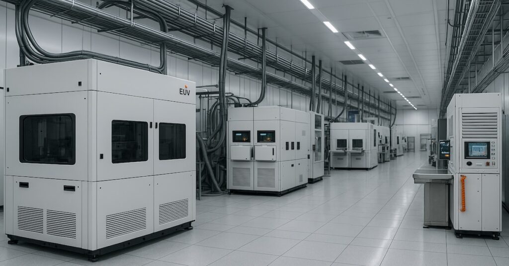
However, this trend reversed in the era of advanced nodes. A recent life-cycle assessment by imec’s Sustainable Semiconductor Technologies program found that cutting-edge processes, such as the A14 node, require multiple patterning and extreme-ultraviolet (EUV) lithography, resulting in energy intensity exceeding 4 kWh/cm². EUV scanners themselves, according to open data on EUV lithography, consume more than 1 megawatt each and use nearly 10 kWh of electricity per wafer pass, over twenty times more than their deep-ultraviolet predecessors.
On the other hand, global energy consumption figures underscore this burden. Azonano’s 2025 industry analysis reported that fabs consumed around 149 billion kWh in 2021, with projections reaching 237 TWh by 2030, levels comparable to the annual electricity demand of a mid-sized nation. The impact of AI is even more dramatic: TechXplore’s reporting noted that AI chip production used 984 GWh in 2024, a 350% increase from the previous year, and could surpass 37,000 GWh by 2030. Meanwhile, SEMI industry reports warn that a single megafab now consumes as much electricity as 50,000 households, while Datacenter Dynamics highlights that TSMC alone accounts for nearly 8% of Taiwan’s electricity use.
In short, scaling has delivered smaller transistors but at the cost of turning modern fabs into some of the largest single consumers of electricity on the planet.
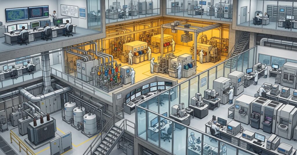
Why Fabs And Tools Consume So Much Power
Building chips at the nanoscale demands extraordinary precision, and that precision comes with enormous energy costs. Modern fabs resemble self-contained cities, running fleets of machines that deposit, etch, inspect, and clean microscopic features while maintaining particle-free environments.
Lithography tools stand out as the biggest energy hogs, but facility systems and even raw material preparation also contribute significantly. The table below highlights how different elements of semiconductor manufacturing stack up in terms of power use and impact.
Taken together, lithography, process equipment, facility systems, and upstream materials explain why fabs are among the most power-intensive industrial facilities in existence.
Each new technology node multiplies the number of steps and tools, pushing power use higher even as individual machines become more efficient.
The race to build faster and more capable chips has delivered extraordinary benefits, but it has also exposed the mounting environmental costs of progress. Moore’s law may evolve, but the laws of thermodynamics remain fixed: every advance demands energy.
In all, the path forward lies in pairing innovation with responsibility, thus prioritizing energy-efficient design, renewable power, and sustainable manufacturing. The choices made today will determine whether future chips are not just smaller and faster, but also cleaner, greener, and more responsible.