Image Generated Using 4o
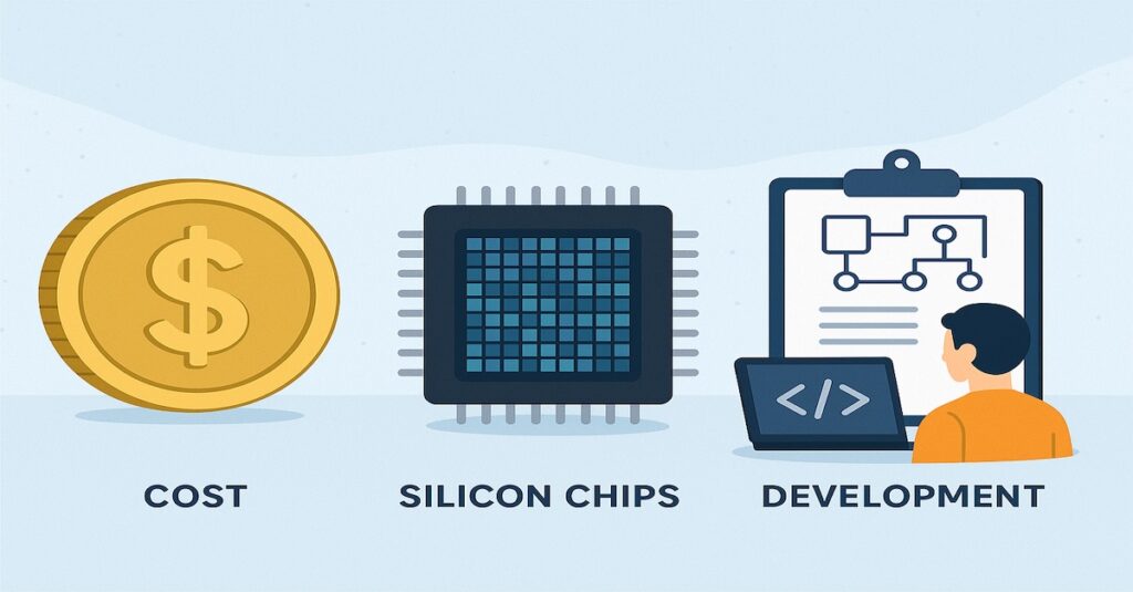
Silicon Alone Is Not The Product
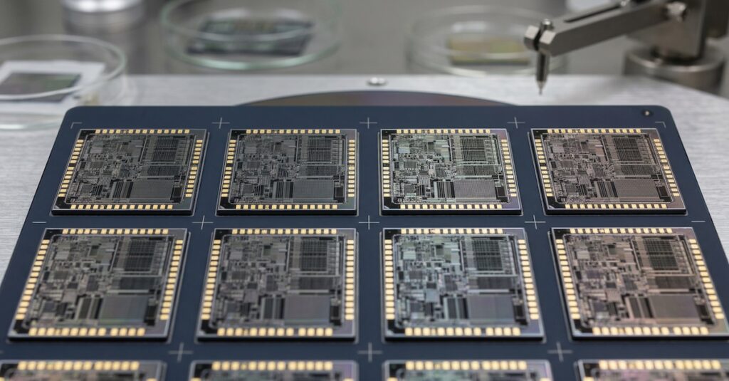
Silicon is the centerpiece of semiconductor innovation, but a bare die is not a product. What comes out of a foundry is an ultra-thin, unprotected sliver of silicon that cannot survive real-world application environments. It lacks mechanical durability, electrical connectivity, and environmental protection. No system designer can solder a raw die onto a board or expose it to industrial use conditions without risking catastrophic failure. The die may contain billions of transistors, but it is inaccessible and incomplete without packaging and interface layers.
The core reasons why silicon is not a finished product:
- It has no standard interface: external signals cannot connect directly to on-die metal pads
- It lacks mechanical protection: dies are prone to cracks, delamination, and ESD damage
- It cannot be mounted: without packaging, there is no board-level attach mechanism
- It is unvalidated: operation under real voltage, temperature, and timing corners remains unknown
- It is unqualified: the die has not passed JEDEC, AEC-Q, or industry-required reliability screening
More importantly, silicon alone does not deliver functionality. Modern chips require configuration, calibration, and system-level interaction before performing as intended. A die sitting in a tray does not regulate power, process data, or handle sensor input. It must be connected to the rest of the system through physical packaging, embedded firmware, and electrical integration. Without this infrastructure, it cannot support its intended use case, let alone pass reliability or performance qualification for commercial deployment.
Ultimately, productization is the bridge between die-level innovation and the end application. Without it, silicon remains a prototype, not a deliverable. The success of a semiconductor product lies not just in its design but in its transformation into a manufacturable, testable, and deployable solution.
Engineering Beyond Silicon
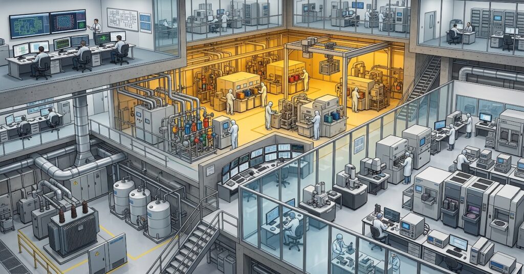
Once the die is fabricated, a deeper engineering phase begins, determining whether the silicon can become a reliable, shippable product. This phase involves translating the raw electrical design into a complete physical and functional unit. It is not enough for the die to meet spec in simulation. It must meet spec in the real world, in every corner case, and under every stress condition. This requires a systematic collaboration between packaging engineers, test engineers, validation teams, and firmware developers.
| Component | Role In Productization |
|---|---|
| Package Design | Determines IO routing, power integrity, and thermal dissipation |
| Test Program Development | Defines coverage, test limits, and pass/fail criteria for each silicon lot |
| Validation Infrastructure | Ensures functionality across PVT (Process, Voltage, Temperature) conditions |
| Qualification Planning | Maps out JEDEC, AEC, or custom reliability tests over production lots |
| Firmware And Calibration | Brings up the chip, configures subsystems, and ensures device consistency |
Yield, Cost, And Time
Even if a chip functions correctly. The success as a product depends on three tightly linked constraints: yield, cost, and time.
High-performance silicon that yields poorly or takes too long to qualify often becomes commercially unviable. Yield losses can occur at multiple stages, such as wafer fabrication, packaging, final test, and system-level integration.
For example, fab defects, package delamination, or test escapes can all degrade the number of good units. At the same time, some failures only emerge under real-world operating conditions like voltage droop or thermal cycling.
A product that yields at 70 percent must absorb that loss into cost, and even modest increases in test time can significantly impact margins at high volumes. Time is equally critical delays in validation or qualification can miss market windows, resulting in lost design wins.
Many chips fail not because they lack functionality but because they cannot meet volume, cost, or launch deadlines. Managing yield, price, and time in semiconductor productization is not optional, it is fundamental to delivering a viable product.
Thinking In Terms Of The Whole Product
A successful semiconductor product is more than a functional die, it results from coordinated engineering across design, packaging, testing, validation, and firmware. Teams that treat tape out as the finish line often face downstream failures that could have been avoided with system-level foresight.
For instance, an SoC with impressive PPA may fail thermal targets due to poor package planning or require silicon respin because debug visibility was not designed. The product mindset starts at architecture, where tradeoffs are made for spec achievement, robustness, yield, and deployment efficiency.
This approach demands that design decisions anticipate real-world constraints: ATE test time limits, handler thermal profiles, firmware bring-up timelines, and qualification windows. It also requires validation environments that reflect actual system use, not just block-level correctness.
Teams considering the whole product build an observability plan for field failures and close the loop between lab data and production metrics. They succeed by designing high-performing silicon and delivering repeatable, validated, and field-ready semiconductor solutions.