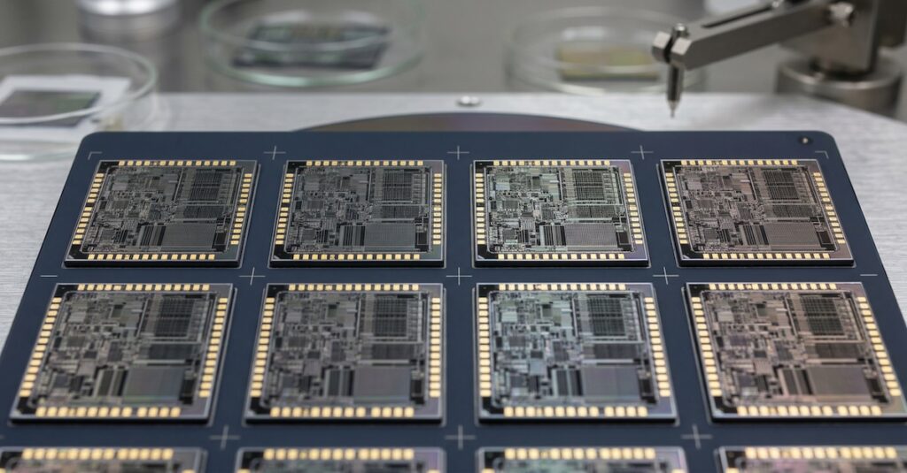
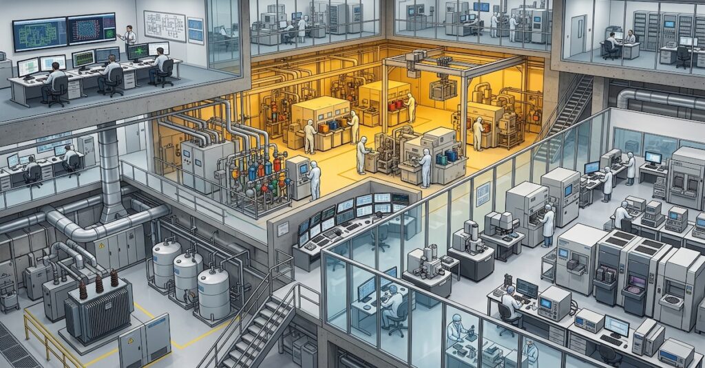
Image Generated Using DALL·E
Semiconductor leadership comes from the lockstep of two strengths: brilliant design and reliable, high-scale manufacturing. Countries that have both move faster from intent to silicon, learn directly from yield and test data, and steer global computing roadmaps.
Countries with only one side stay dependent, either on someone else’s fabs or on someone else’s product vision.
Extend the lens: when design and manufacturing sit under one national roof or a tightly allied network, the feedback loop tightens. Real process windows, such as lithography limits, overlay budgets, CMP planarity, and defectivity signatures, flow back into design kits and libraries quickly. That shortens product development cycles, raises first pass yield, and keeps PPA targets honest. When design is far from fabs, models drift from reality, mask rounds multiply, and schedules slip.
In all, semiconductor leadership comes from the lockstep of two strengths: brilliant design and reliable, high-scale manufacturing.
Countries that combine both move faster from intent to silicon, learn directly from yield and test data, and steer global computing roadmaps. At the same time, those with only one side remain dependent on someone else’s fabs or someone else’s product vision.
A nation strong in design but weak in manufacturing faces long debug loops, limited access to advanced process learning, and dependence on external cycle times. A nation strong in manufacturing but with a focus on design, the light industry depends on external product roadmaps, which slows learning and dampens yield improvements. The durable edge comes from building both and wiring them into one disciplined, high-bandwidth, technical feedback loop.
Let us take a quick look at the design and manufacturing lens from country point of view.
The Design
A strong design base is the front-end engine that pulls the whole ecosystem into orbit. It creates constant demand for accurate PDKs, robust EDA flows, MPW shuttles, and advanced packaging partners, shrinking the idea-to-silicon cycle. As designs iterate with honest fab feedback, libraries and rules sharpen, startups form around reusable IP, and talent compounds.
| Mechanism | Ecosystem Effect |
|---|---|
| Dense design clusters drive MPW shuttles, local fab access, advanced packaging, and test | Justifies new capacity; lowers prototype cost and time |
| Continuous DTCO/DFM engagement with foundries | Faster PDK/rule-deck updates; higher first-pass yield |
| Reusable IP and chiplet interfaces | Shared building blocks that accelerate startups and SMEs |
| Co-located EDA/tool vendors and design services | Faster support, training pipelines, and flow innovation |
| University–industry, tape-out-oriented programs | Steady talent supply aligned to manufacturable designs |
When design is strong, the country becomes a gravitational hub for tools, IP, packaging, and test. Correlation between models and silicon improves, respins drop, and success stories attract more capital and partners, compounding advantage across the ecosystem.
The Manufacturing
Manufacturing is the back-end anchor that turns intent into a reliable product and feeds complex data back to design. Modern fabs, advanced packaging lines, and high-coverage test cells generate defect maps and parametric trends that tighten rules, libraries, and package kits. This credibility attracts suppliers, builds skills at scale, and reduces the risk associated with ambitious roadmaps.
| Mechanism | Ecosystem Wffect |
|---|---|
| Inline metrology, SPC, and FDC data streams | Rapid rule-deck, library, and corner updates for design |
| Advanced packaging (2.5D/3D, HBM, hybrid bonding) | Local package PDKs; chiplet-ready products and vendors |
| High-throughput, high-coverage test | Protected UPH; earlier detection of latent defects; cleaner ramps |
| Equipment and materials supplier clustering | Faster service, spare access, and joint development programs |
| Scaled technician and engineer training | Higher uptime; faster yield learning across product mixes |
With strong manufacturing, ideas become wafers quickly, and learning cycles compress. Suppliers co-invest, workforce depth grows, and the feedback loop with design tightens, creating a durable, self-reinforcing national semiconductor advantage.
A nation that relies solely on design or solely on manufacturing invites bottlenecks and dependency. The edge comes from building both and wiring them into a fast, disciplined feedback loop so that ideas become wafers, wafers become insight, and insight reshapes the next idea.
When this loop is tight, correlation between models and silicon improves, mask reentries fall, first pass yield rises, and ramps stabilize sooner.


