Image Generated Using 4o
The Data Explosion Across The Semiconductor Lifecycle
The semiconductor industry has always been data-intensive. However, the conversation is now shifting from quantity to quality. It is no longer about how much data we generate, but how well that data is connected, contextualized, and interpreted.
Semiconductor data is fundamentally different from generic enterprise or consumer data. A leakage current reading, a fail bin code, or a wafer defect has no meaning unless it is understood in the context of the silicon process, test environment, or design constraints that produced it.
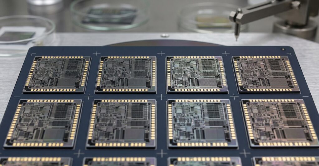
In the early stages of product development, design engineers generate simulation data through RTL regressions, logic coverage reports, and timing closure checks. As that design progresses into the fabrication phase, silicon data begins to accumulate, including inline metrology readings, critical dimension measurements, tool state logs, and wafer-level defect maps. Each wafer and lot carries a unique signature, influenced by upstream process variability and tool interactions.
By the time the product reaches assembly and packaging, new forms of data emerge. Material-level stress tests, warpage analysis, and thermal cycling behavior contribute additional layers that directly influence the chip’s electrical characteristics. Test data provides even more clarity, offering per-die measurement results, analog waveforms, and bin distributions that give a definitive verdict on performance.
What often gets overlooked is field and reliability data. Customer returns, in-system failures, or aging trends can reveal issues not caught during qualification, but only if they are traceable to original silicon and test metadata. This level of visibility requires not only data collection but also a deep integration of context across multiple lifecycle stages.
When this information is viewed in fragments, it remains passive. However, when connected across design, fabrication, test, and field, with the help of domain expertise and timing correlation, it becomes a powerful driver of yield learning, failure analysis, and operational improvement.
Why This Data Explosion Matters And What The Future Holds
Historically, many semiconductor decisions relied on engineering experience and past norms. That worked when processes were simpler and product diversity was limited. However, today’s environment involves complex interactions among design, process, and packaging, often monitored through hundreds of sensors per wafer and analyzed across multiple-site operations. In this landscape, judgment alone is no longer sufficient.
Semiconductor data without context quickly becomes noise. Engineers are now expected to interpret results from thousands of bins, multiple product variants, and evolving test conditions. The complexity has outpaced manual tracking, and the risk of subtle, systemic failures has increased. A defect might only surface under extreme conditions, such as thermal, voltage, or frequency extremes, and often only becomes visible when data from design, fabrication, and testing are brought together.
Modern yield learning relies on this integration. Identifying the root cause of a parametric drift may involve tracing back through etch step uniformity, layout geometry, and even packaging stress. Product decisions, such as qualifying a new foundry or modifying test content, now require simulations and data modeling based on historical silicon behavior. The accuracy and speed of these decisions are directly tied to how well the data is connected.
Looking ahead, the role of data will become even more critical. Real-time adjustments within fab and test operations, AI-assisted diagnostics built on die-level signatures, and traceability frameworks linking field failures back to initial silicon lots are becoming standard. The goal is not just to collect data, but to create systems where decisions adapt continuously based on reliable, context-aware insights.
| Tool Type | Primary Purpose |
|---|---|
| EDA Analytics Platforms | Analyze simulation logs, coverage gaps, layout issues, and IP reuse patterns |
| Yield Management Systems (YMS) | Detect wafer-level spatial defects, monitor process trends, and bin correlations |
| Manufacturing Execution Systems | Track wafer routing, tool excursions, process skips, and inline inspection logs |
| Test Data Analysis Platforms | Aggregate multisite ATE results, identify failing die clusters, and escape risks |
| Data Lakes and Pipelines | Centralize structured/unstructured data across fab, test, and reliability stages |
| BI Dashboards & Statistical Tools | Present KPI trends, failure rates, and yield performance to engineering teams |
Types Of Tool Enabling The Data-Driven Flow
The move toward data-driven decisions in semiconductors is only possible because of an expanding class of specialized tools. These tools are built not just to process data, but to respect the context of semiconductor manufacturing, where each decision is linked to wafer history, test condition, and physical layout.
Unlike generic enterprise systems, semiconductor tools must track process lineage, equipment behavior, lot IDs, and die-level granularity across globally distributed operations. The result is a layered, highly domain-specific tooling stack.
Integration remains the hardest part. Viewing a failing wafer map is one thing, linking that map to a specific process drift or a marginal scan chain requires a seamless connection between these tools. As this ecosystem matures, the goal is no longer just to collect and display data but to make it actionable across teams and timeframes.
Ultimately, the strength of any data system is not in the software alone but in how effectively engineers use it to ask the right questions and drive better outcomes.
Skills For The Data-Driven Semiconductor Era
As semiconductor operations become more data-centric, the skills required to succeed are evolving. It is no longer enough to be an expert in one domain. Engineers and managers must now understand how to interpret complex datasets and act on them within tight product and business timelines.
The ability to work with silicon and chip data, coupled with the judgment to understand what the data means, is quickly becoming a core differentiator across roles.
| Skill Category | Description | Where It Matters Most |
|---|---|---|
| Data Contextualization | Understanding where data comes from and how it ties to process steps, design intent, or test | Yield analysis, silicon debug, test correlation |
| Tool Proficiency | Working fluently with tools like JMP, Spotfire, YieldHub, Python, SQL, Excel VBA, or cloud dashboards | ATE debug, failure analysis, KPI reporting |
| Statistical Reasoning | Applying SPC, distributions, hypothesis testing, variance analysis, regression models | Process tuning, guardband optimization, lot release criteria |
| Cross-Functional Thinking | Bridging design, fab, test, packaging, and field return data | Automotive, aerospace, high-reliability segments |
| Traceability Awareness | Linking test escapes or RMAs to silicon history, probe card changes, or packaging issues | Reliability, RMA teams, quality control |
| Decision Framing | Converting data into business-impacting insights and prioritizing next actions | Product and test managers, program owners |
| Data Cleaning and Wrangling | Detecting and correcting anomalies, formatting raw logs, aligning inconsistent sources | ATE log analysis, fab tool monitoring, multi-LOT reviews |
| Root Cause Pattern Recognition | Recognizing recurring patterns across electrical and physical data layers | Failure debug, device marginality analysis |
| Visualization and Reporting | Building dashboards or visuals that accurately summarize issues or trends | Weekly yield reviews, executive reports, test program signoff |
| Data Governance Awareness | Understanding data security, version control, and access in shared environments | Shared vendor ecosystems, foundry engagements |
| AI/ML Familiarity | Recognizing where AI models can assist in diagnostics or decision support | Predictive maintenance, smart binning, parametric modeling |
These skills are not replacements for engineering fundamentals and they are extensions. An engineer who can ask better questions of the data, challenge its quality, or trace it to the right source is far more valuable than someone who simply views a chart and moves on.
As data continues to becomes core to every semiconductor engineering judgment, the ability to understand, shape, and explain that data will define the next generation of semiconductor professionals.