Image Generated Using Nano Banana
The End Of Architectural Consensus
The semiconductor industry is undergoing a fundamental architectural break. For over 50 years, general-purpose computing has prevailed thanks to software portability, transistor-driven scaling, and the absence of workloads that demanded radical alternatives. That era is over.
With Moore’s Law slowing to single-digit gains and Dennard scaling effectively dead, the hidden energy and performance subsidy that made CPUs “good enough” has vanished. Meanwhile, AI workloads now require 100x to 10,000x more compute than CPUs can provide economically, forcing a shift to purpose-built architectures.
What has changed is not that specialized processors are faster, which has always been true, but that the performance gap is now so large it justifies ecosystem fragmentation and platform switching costs.
Specialized architectures win because their optimizations compound. They align parallelism with workload structure, tune memory access patterns, scale precision to algorithmic tolerance, and embed domain-specific operations directly in hardware.
These advantages multiply into 10,000x efficiency improvements that approach thermodynamic limits. General-purpose chips cannot close that gap, regardless of how many transistors they add.
Vertical Integration For Purpose-Specific Silicon Design
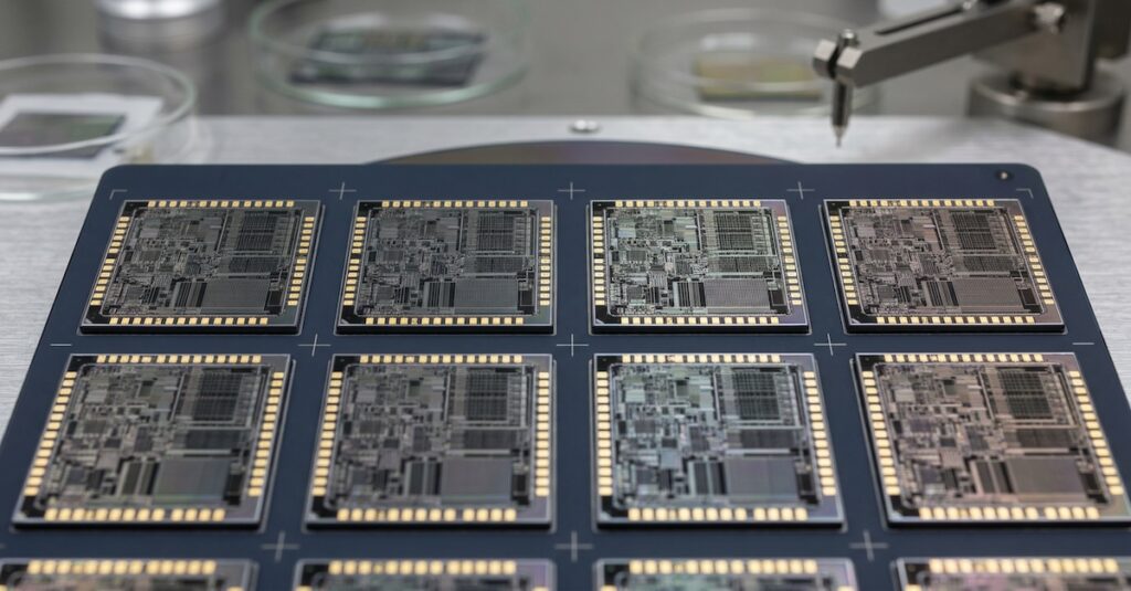
The shift toward custom silicon marks one of the most consequential strategic pivots in modern computing. For decades, the industry relied on merchant silicon vendors to supply general-purpose processors, enabling broad ecosystem access and a relatively level competitive field. That balance is now collapsing.
When companies like Google, Amazon, and Meta invest billions to design their own chips, once the domain of specialized semiconductor vendors, they are not simply optimizing compute units. They are vertically integrating the computational stack.
The table below describes the mechanism and path by which vertical integration in silicon is leading to the reconcentration of computing power:
| Phase | Compute Architecture Model | Silicon Strategy | Core Capability Requirements | Where Value Is Captured | Industry Structure |
|---|---|---|---|---|---|
| Phase 1 | General Purpose Computing | Merchant silicon | Procurement, standardization, software portability | Chip vendors, CPU platforms | Broad, horizontal, open ecosystem |
| Phase 2 | Accelerated Computing (GPU era) | Domain-optimized accelerators | Parallel programming models, runtime frameworks | Silicon + software stacks | Early signs of consolidation |
| Phase 3 | AI-Native Compute Platforms | Light customization, firmware-level tuning | Packaging, interconnect tuning, software toolchains | Silicon + compiler + runtime | Compute access becomes bottleneck |
| Phase 4 | Vertically Integrated Compute | In-house or deeply co-designed accelerators | Architecture, EDA, compiler, systems design | Silicon + system + cloud economics | Advantage shifts to those controlling full stack |
| Phase 5 | Silicon-Native Infrastructure | Full-stack co-optimization: chip, system, workload | Algorithm + hardware co-design, multi-year roadmaps | End-to-end platform control | Reconcentration, winner-take-most dynamics |
The economic logic is clear: even small efficiency gains, measured in single-digit percentage improvements, translate into hundreds of millions in savings when spread across millions of processors and tens of thousands of AI clusters.
At the same time, custom silicon enables performance and efficiency profiles that off-the-shelf solutions cannot match. The result is not just faster chips, but the ability to architect entire data centers, scheduling systems, memory fabrics, and cooling environments around silicon they control years in advance.

The Two-Tier Computing Economy And Consequences
A structural divide has emerged in modern computing, characterized by a two-tier computing economy, where traditional workloads continue to run efficiently on commodity CPUs. At the same time, AI and frontier applications require specialized accelerators that general-purpose processors cannot support.
This split mirrors the evolution of high-performance computing, where systems like Frontier had no choice but to adopt thousands of GPU accelerators to reach exascale within power and cost constraints.
The same dynamic now extends beyond HPC. Apple Silicon demonstrates how custom chips deliver performance-per-watt advantages that are impossible with merchant x86 processors, while Tesla’s autonomous driving processors show that real-time AI inference under tight thermal limits demands entirely new silicon architectures.
The consequence is a computing landscape divided by capability, economics, and accessibility. Those with the scale, capital, and technical depth to design or co-design silicon gain access to performance and efficiency unattainable through merchant hardware.
Everyone else must either rent access to specialized accelerators through hyperscalers, creating a structural dependency, or remain constrained to slower, less efficient CPU-based systems.
In effect, computing is entering a new era where advanced capabilities are increasingly concentrated, echoing the mainframe era but now driven by AI, thermodynamics, and silicon control at a planetary scale.

Strategic Implications And The Post-General-Purpose Landscape
As computing splinters into purpose-specific architectures, the tradeoff between optimization and portability becomes unavoidable. The collapse of the “write once, run anywhere” model forces developers to choose between sacrificing up to 30 to 90 percent of potential performance on general-purpose hardware or investing in architecture-specific optimization that fragments codebases.
In AI alone, models running unoptimized on CPUs can perform 50 to 200 times slower than on accelerators designed for tensor operations. Every new accelerator also demands its own toolchains, compilers, profilers, and programming abstractions. This is why companies now spend more on their AI engineering effort adapting models to specific silicon targets, rather than improving the models themselves.
The economics create a structural divide. Custom silicon becomes cost-effective only at a massive scale, typically involving one to three million deployed processors, or under extreme performance constraints such as autonomous driving or frontier AI training. Below that threshold, organizations must rely on cloud accelerators, locking them into hyperscaler pricing and roadmaps. The strategic dimension is equally clear.
Control over custom silicon provides supply security and technology sovereignty, especially as export controls and geopolitical friction reshape semiconductor access. The result is a rapidly diverging compute landscape. Innovation accelerates as specialized architectures explore design spaces that general-purpose CPUs never could.
Still, the cost is a fragmented ecosystem and a concentration of computational power among those with the scale, capital, and silicon capability to shape the post-general-purpose era.