Image Generated Using DALL-E
Prototyping Is Not A Production
Scaling a semiconductor design from prototype to production is where promising ideas meet harsh reality. A prototype demonstrates feasibility and shows that a concept can work under controlled conditions but is not a finished product. Many teams celebrate the first silicon success, only to realize later that this milestone marks the beginning of the journey to market, not the end.
The challenges of scaling are often underestimated. At advanced nodes, a single complete mask set can cost upward of a million dollars. A seemingly minor design change, such as adjusting a clock buffer or modifying a pin assignment, can require a complete mask revision and push schedules back by several weeks.
On the other hand, custom test boards, essential for silicon bring-up and debugging, often cost hundreds of thousands of dollars per iteration, depending on complexity. Then, the debug cycles after prototype validation, whether addressing signal integrity issues, timing violations, or power delivery concerns, can add four to eight weeks per iteration.
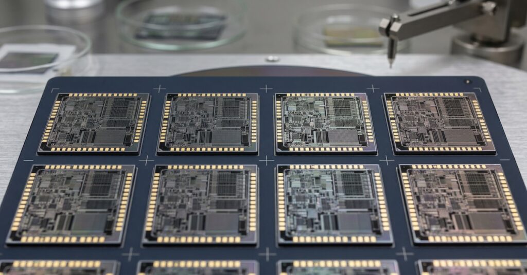
Prototypes often rely on multi-project wafer shuttles to reduce early costs, but these shared runs offer only a limited view of production readiness. They do not reflect the true complexity of dedicated wafer starts, volume scaling, or the demands of final test and qualification. A prototype proves that a design can function in the lab but does not guarantee manufacturability, stable yield, or long-term reliability in a production environment.
This gap between a working design and a shipping product is where the real cost of scaling is revealed.
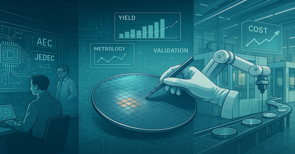
Cost Of Prototyping
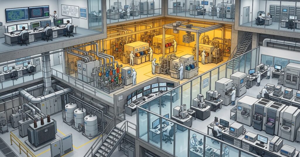
Prototyping is the first critical milestone in the semiconductor New Product Introduction (NPI) process. It is much more than demonstrating that a design works on paper. A prototype integrates silicon fabrication, hardware development, test program creation, and validation under real-world conditions.
Each step introduces risk, consumes resources, and requires precise coordination. Early success with a prototype can create the impression that a design is ready for production, but this is often misleading.
A functioning prototype does not ensure the design will meet yield, reliability, and manufacturability targets in volume. The complexity of scaling is frequently underestimated, leading to unexpected delays, rework cycles, and increased costs.
| Activity | Typical Timeframe | Cost Considerations |
|---|---|---|
| Mask Set Development | 4 to 6 weeks | High fixed cost per iteration |
| Multi-Project Wafer (MPW) Shuttle | 3 to 4 months availability | Lower cost, limited production insight |
| Test Board Design and Fabrication | 3 to 5 weeks | Multiple iterations may be required |
| ATE Test Program Development | 4 to 6 weeks | Tester time and engineering effort |
| PVT Characterization | 3 to 5 weeks | Requires multiple wafer lots |
| Qualification (JEDEC, AEC) | 8 to 12 weeks | Full wafer lots, package variants, and extended testing |
| Debug and Correlation Cycles | 2 to 4 weeks per issue | Additional wafer use and test time |
The path from prototype to production demands a tightly managed flow that balances silicon development, board design, test engineering, and system validation. Minor design changes can trigger costly and time-consuming rework. At the same time, late-stage discoveries of signal integrity issues, timing violations, or power delivery challenges can set entire programs back by weeks or months.
Prototypes typically rely on shared wafer shuttles and lab setups that do not reflect the realities of dedicated high-volume production. Without a robust plan for test coverage, validation, and correlation, teams risk entering production with incomplete knowledge of their design’s behavior.
A successful prototype results from cross-functional alignment between design, hardware, and validation teams. When this coordination breaks down, the actual cost of prototyping reveals itself in missed schedules, strained budgets, and compromised product launches.
Transitioning To Production
Transitioning a semiconductor design from prototype to production is not a simple handoff. It is a complex, iterative process that requires carefully coordinating design teams, manufacturing partners, test engineers, and supply chain specialists.
What works in a lab must now perform reliably across millions of units. This step demands a shift in mindset from optimizing for a single working chip to building a repeatable, scalable process that delivers consistent performance and yield.
Production readiness hinges on a deep understanding of the entire flow. Foundry slots must be secured based on realistic forecasts, and wafer starts must align with packaging and test capacity. Any misalignment in this chain introduces delays that ripple across the schedule.
For example, a late-stage design change can trigger a new mask spin, delay wafer starts, and require revalidation of test programs and packaging processes. Each step consumes time and resources, creating a compounding effect that can push out delivery timelines and strain customer relationships.
Transitioning to production is not just about pushing more wafers through a fab. It is about building a reliable, predictable system that balances technical rigor with operational efficiency. Success at this stage determines whether a design remains an engineering milestone or becomes a commercially viable product.
Takeaway
Scaling a semiconductor design from prototype to production is a complex, multi-dimensional challenge. A design must not only work in a lab but also withstand the realities of high-volume manufacturing, tight supply chains, and demanding customer timelines.
The costs and risks involved at each stage, from mask sets and test infrastructure to packaging yield and logistics, compound quickly. Small inefficiencies in yield or test throughput can multiply into significant financial losses when measured across millions of units.
Success in semiconductor scaling is not the result of technical brilliance alone. It is built on operational discipline, proactive risk management, and cross-functional alignment across design, manufacturing, and supply chain teams.
Teams that plan for the entire journey anticipate challenges and maintain a deep focus on execution, ultimately succeeding in turning innovative designs into commercially viable products.