Image Generated Using 4o
AI Workloads Redefine Chip Architecture
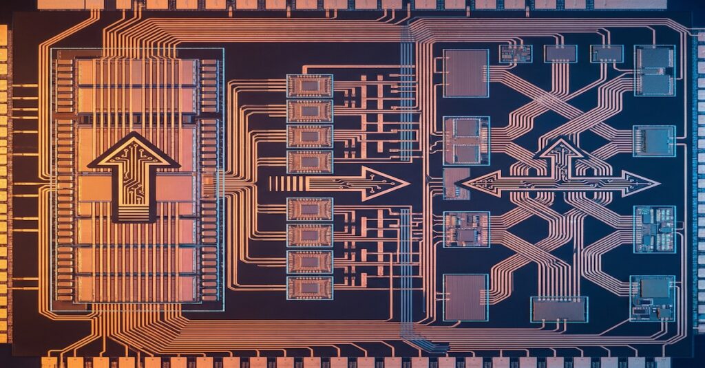
AI workloads are fundamentally different from traditional computing tasks. Where classic CPUs focused on serial instruction execution, AI models and intense neural networks demand massive parallelism and high data throughput. This has driven a shift toward specialized compute architectures, such as GPUs, tensor processors, and custom AI ASICs. These designs move away from pure von Neumann principles, emphasizing data locality and minimizing costly data movement.
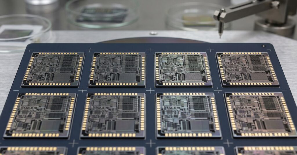
At the heart of this shift is the need to process billions of operations efficiently, for which the traditional architectures struggle to meet AI’s bandwidth and memory requirements, leading designers to adopt local SRAM buffers, near-memory compute, and advanced interconnects. However, these improvements come at the cost of larger die areas, power density challenges, and significant NRE costs, particularly on advanced nodes.
For customers, these changes present both opportunities and risks. Custom AI silicon offers significant performance and power advantages, but it requires deep expertise in hardware-software co-design and substantial upfront investments. While hyperscalers and large OEMs pursue custom ASICs for competitive differentiation, smaller players often remain on general-purpose GPUs to avoid high development costs and longer time-to-market.
Ultimately, AI workloads are reshaping not only chip architectures but the economics of semiconductor design. The rapid pace of AI model evolution forces designers to iterate through silicon cycles at a high frequency, placing immense pressure on design teams, foundries, and the entire supply chain. While the industry stands to benefit enormously from AI-driven demand, it must navigate growing complexity, power limits, and escalating costs to deliver sustainable innovation in the years ahead.
Impact On Process Nodes And Technology Roadmaps
AI has also become a significant force shaping process technology roadmaps. Unlike previous drivers, such as mobile or standard compute, AI accelerators require enormous compute density and power efficiency. Advanced nodes, ranging from 7nm to 2nm, are attractive because they offer higher transistor performance, improved energy efficiency, and increased integration capabilities, all of which are critical for massive AI workloads.
However, these benefits come with significant trade-offs, including escalating design costs, more complex manufacturing, and tighter control over variability.
| Node | Key AI Benefits | Main Challenges | Typical AI Use Cases |
|---|---|---|---|
| 7nm | Good density and performance; mature yields | Power still high for very large chips | Mid-size AI accelerators, edge AI SoCs |
| 5nm | Better energy efficiency; higher transistor count | Rising mask costs; increased design rules complexity | High-performance inference, initial LLM training |
| 3nm | Significant performance gains; lower power | Yield variability; extreme design complexity | Large AI ASICs, data center accelerators |
| 2nm | Advanced gate structures (nanosheet/GAA); excellent scaling | Immature yields; highest costs; thermal density | Cutting-edge AI training, future LLM architectures |
These technology nodes are crucial enablers for achieving AI performance targets, but they also exponentially increase costs. Mask sets touches million at 3nm and beyond, making custom AI silicon viable only for companies with significant scale or unique workloads. At the same time, the physical limits of power density mean that merely shrinking transistors is not enough. Advanced cooling, power delivery networks, and co-optimized software stacks are now mandatory to fully realize the benefits of smaller nodes.
As a result, the AI revolution is not just accelerating node transitions but fundamentally changing how companies think about chip design economics. To tackle this, the industry is moving toward chiplet architectures, heterogeneous integration, and tight hardware-software codesign to balance performance gains against skyrocketing complexity and costs.
Overall, AI is no longer simply an application. It is also shaping the entire technology roadmap for the semiconductor industry.
Supply Chain And Manufacturing Pressure
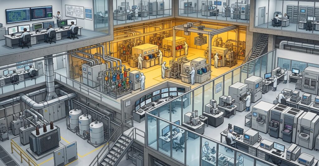
The AI boom has also exposed significant bottlenecks across the semiconductor supply chain. Unlike typical semiconductor products, AI accelerators are extremely large, power hungry, and require advanced packaging and memory technologies. These characteristics have placed unprecedented strain on fabrication capacity, substrate availability, advanced packaging lines, and test infrastructure.
The global shortages of GPUs over the past two years are a direct consequence of these constraints, compounded by the explosive demand for AI and limited manufacturing flexibility for such specialized devices.
| Supply Chain Area | AI-Driven Challenges | Impacts |
|---|---|---|
| Foundry Capacity | AI chips demand leading-edge nodes (5nm, 3nm), consuming large die areas and reticle-limited designs. | Limited wafer starts for other segments; long lead times; higher wafer costs. |
| Substrate Manufacturing | Large interposers needed for chiplets and HBM; organic substrate capacity under strain. | Shortages of ABF substrates; increased substrate costs; delivery delays. |
| Advanced Packaging | 2.5D/3D integration (e.g. CoWoS, Foveros) essential for AI chips. | OSAT capacity constrained; long cycle times; thermal and yield challenges. |
| Testing Infrastructure | Large AI devices have complex test vectors; high power complicates burn-in and functional test. | Longer test times; increased test costs; limited availability of high-power ATE equipment. |
| HBM Memory Supply | AI accelerators increasingly rely on HBM2e, HBM3; production is concentrated among few vendors. | Supply constraints limit AI chip output; significant cost increases for HBM stacks. |
| Equipment Availability | EUV lithography tools are limited in number and expensive to deploy. | Throughput constraints slow ramp of advanced nodes; high capital requirements. |
| EDA Tool Scalability | AI chip designs are extremely large (hundreds of billions of transistors). | Longer place-and-route times; higher tool licensing costs; increased verification complexity. |
| Material Supply Chain | Advanced processes require ultra-pure chemicals and specialty materials. | Vulnerable to geopolitical risks; localized shortages can halt production. |
Foundry capacity has become a significant bottleneck for AI chips, which often require large die sizes close to reticle limits. These large designs consume significant wafer starts, increasing defect risks, yield challenges, and lead times, while driving higher costs and capacity reservations from major AI players.
Advanced packaging is equally strained. AI designs rely on chiplets and high-bandwidth memory stacked with interposers, requiring complex processes such as CoWoS and Foveros. Substrate shortages and specialized test needs further slow production, as large AI chips require high power handling and complex validation.
Overall, AI has exposed deep vulnerabilities in semiconductor manufacturing. Without significant expansion in lithography, packaging, and test capacity, these bottlenecks will continue to constrain the speed at which AI solutions can reach the market, impacting their cost and availability.
Long-Term Implications For Industry Economics And Design
AI is also fundamentally transforming how the semiconductor industry thinks about both business economics and technical design. Unlike traditional markets like mobile or PCs, which relied on massive volumes to justify advanced-node costs, AI silicon often serves lower-volume segments with extremely high chip complexity and premium pricing.
This disrupts the traditional model of spreading non-recurring engineering (NRE) costs over millions of units and forces companies to weigh the risks and rewards of investing in custom hardware for rapidly evolving AI workloads.
The net result is an industry facing higher costs, faster technical cycles, and the need for closer collaboration between silicon engineers and AI software teams. While AI promises significant new opportunities, it also raises the stakes for semiconductor companies, demanding greater agility, investment, and technical depth to remain competitive in this rapidly shifting landscape.