Image Generated Using DALL·E
Rising Energy Burden Of Lithography
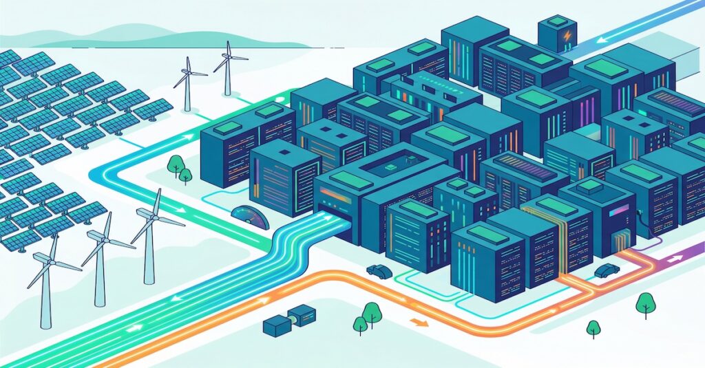
Lithography has become one of the most energy-intensive stages in the fabrication of wafers. As fabs push to 2 nm and below, every additional patterning layer increases electricity demand and associated CO₂ emissions. Industry projections now indicate that wafer-fab emissions will exceed approximately 270 Mt CO₂e by 2030, primarily from equipment-driven loads. Fabs cannot treat lithography power as a fixed cost anymore.
High-NA EUV, expected to be widely deployed in high-volume environments, delivers the resolution needed for advanced logic. However, it also increases per-tool power requirements, precisely the kind of “performance/energy ↑” tradeoff that sustainability teams are trying to mitigate. This imbalance is the reason lithography is now being singled out in sustainability roadmaps.
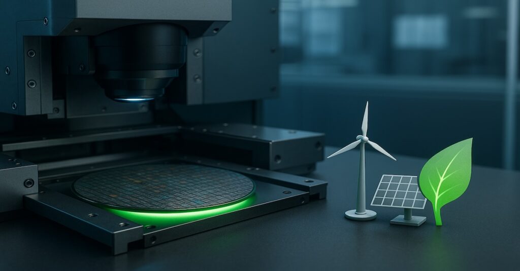
What “Energy-Aware” Really Means
Energy-aware lithography integrates power consumption as a design and operational variable within the patterning process, alongside resolution, critical dimension control, and throughput. Instead of viewing electricity as a fixed cost, it measures kWh per wafer and CO₂ per layer as core performance metrics. Each exposure plan and dose setting is evaluated for both imaging fidelity and energy efficiency, shifting lithography from precision alone to precision with purpose.
At the fab level, energy awareness spans scanner design, standby control, and load balancing across exposure tools. It links process control with power management, allowing for the precise achievement of exact yield and overlay targets with reduced energy consumption. In this framework, sustainability becomes an engineered outcome rather than an afterthought.

Emerging Data From Recent Research
Recent years have seen semiconductor research institutions and equipment makers quantify lithography’s energy and carbon footprint with far greater precision. This shift from broad sustainability targets to verifiable metrics such as energy per wafer, kilowatt-hours per layer, and carbon dioxide equivalent per exposure has redefined how efficiency is measured.
Organizations such as imec, ASML, and TSMC now publish data showing measurable progress in reducing power consumption across both process and equipment levels, aligning with the 2024 IRDS Environmental Chapter, which calls for quantifiable energy tracking throughout semiconductor manufacturing.
At the same time, policy frameworks such as NIST’s 2024 environmental assessment and SRC’s sustainability initiatives have recognized tool-level efficiency as a direct lever for emission reduction. This alignment between research, industry reporting, and regulatory guidance represents the first coordinated movement toward energy-transparent lithography, where every exposure and patterning decision is tied to a measurable energy outcome.
| Paper Title | Year And Paper Link | Summary And Relevance |
|---|---|---|
| Toward Lifelong-Sustainable Electronic-Photonic AI Hardware | 2025 arXiv | Highlights that for cutting-edge chips the embodied carbon (including lithography/EUV) is growing even as operational efficiency improves. Useful for framing lithography’s sustainability burden. |
| Carbon Per Transistor (CPT): The Golden Formula for Sustainable Semiconductor Manufacturing | 2025 arXiv | Presents a quantitative model of semiconductor fabrication carbon footprint, highlighting that lithography (with other front-end steps) dominates wafer-fab emissions. |
| Can we improve the energy efficiency of EUV lithography? | 2024 arXiv | Directly addresses EUV lithography power consumption and suggests routes to reduce source power by an order of magnitude, highly relevant for your lithography-energy theme. |
| Modeling PFAS in Semiconductor Manufacturing to Quantify Trade-offs in Energy Efficiency and Environmental Impact of Computing Systems | 2025 arXiv | While focused on PFAS (materials), this paper also touches on patterning complexity (incl. lithography) and embodied carbon/material trade-offs, useful to show the broader sustainability context. |
| Carbon Connect: An Ecosystem for Sustainable Computing | 2024 arXiv | Discusses large-scale manufacturing, including semiconductor fabs’ electricity usage (comparable to datacenters) and mentions extreme ultraviolet lithography in that context. |
| How purity reshapes the upstream materiality of semiconductor manufacturing | 2025 arXiv | Addresses supply-chain/material dependencies for lithography (e.g., neon/argon gases for excimer lasers) and helpful to show indirect energy/material burdens tied to lithography. |
Recent studies from imec, ASML, and TSMC, supported by analyses such as Shintake (2024) on EUV power reduction and ElSayed et al. (2025) on carbon-per-transistor metrics, show a clear shift in how lithography energy is being addressed. The emphasis has moved from large facility upgrades to tool- and process-level optimization, where adaptive standby control, exposure planning, and dose tuning yield immediate reductions in power use.
Together, these works demonstrate that lithography energy is now a quantifiable engineering parameter. Integrating power metrics into process control and equipment specifications turns sustainability into a driver of performance, advancing the concept of truly energy-aware semiconductor manufacturing.
Toward A Metric Of Energy Transparency
Latest developments across the industry have also highlighted a growing focus on the transparent reporting of lithography energy use. ASML has disclosed that its NXE:3600D EUV systems consume about 7.7 kilowatt-hours per exposed wafer pass, offering a concrete reference point for equipment-level efficiency.
IMEC’s modeling work indicates that lithography and etch together contribute over 40 percent of Scope 1 and 2 carbon emissions at advanced logic nodes, emphasizing where process-level optimization delivers the most significant impact. TSMC’s EUV Dynamic Power Saving Program further demonstrates operational transparency by achieving a 44 percent reduction in peak power and projecting 190 million kilowatt-hours in energy savings by 2030.
These examples collectively point toward a future where lithography energy is treated as a measurable parameter rather than an indirect cost. Adopting standard metrics, such as kilowatt-hours per exposure or carbon-equivalent per layer, would allow fabs and equipment suppliers to benchmark their performance and optimize power alongside yield and throughput.
Energy transparency at this level establishes efficiency as a shared engineering objective across the semiconductor ecosystem.