Photo by Maxence Pira on Unsplash
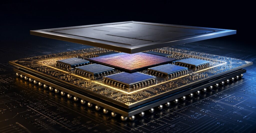
The semiconductor node is the most vital technical topic in the semiconductor industry. Technology node forms the basis for developing different types of silicon products. Over the last decade, top semiconductor manufacturers have invested a lot of time and capital to bring new semiconductor technology nodes.
Such push is due to two critical aspects. The first one is technical, as it focuses on bringing new advanced solutions to the market. The second one is more business-oriented, where the manufacturers bring new capacity to manage future demand.
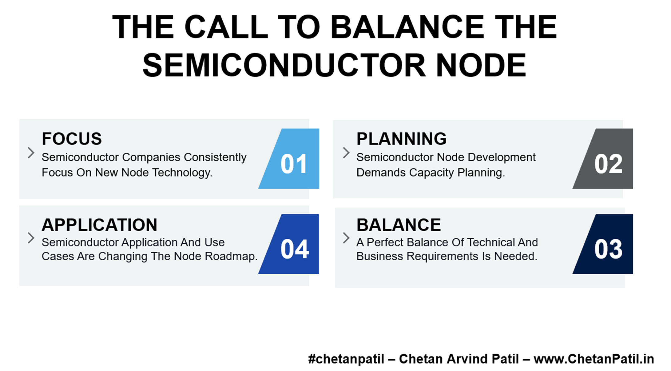
Focus: Semiconductor Companies Consistently Focus On New Node Technology.
Planning: Semiconductor Node Development Demands Capacity Planning.
Eventually, the demand for a specific technology node is due to the market and application use cases. However, even with all the available data about how the consumer market will grow, there is still a gap between the type of technology node capacity.
This gap is due to the focus on bringing capacity for the matured technology. It is a logical step given the need to cater to different system applications that still rely on such technology nodes. On the other side, to ensure future demand for advanced nodes is met, there needs to be a balance in semiconductor fabrication capacity.
To bring the balance in semiconductor technology nodes, not only manufacturers should plan and invest, but public bodies also need to provide the required incentives and policies impetus. Several of the advanced semiconductor node FABs are only possible due to support from government bodies.
The current view of semiconductor FAB type clearly shows that the 200nm wafer FABs are dominant. Within 200nm FABs, matured technology capacity share is more than 30-40%. It is due to the market requirements and the need to support legacy products.
Balance: A Perfect Balance Of Technical And Business Requirements Is Needed.
Application: Semiconductor Application And Use Cases Are Changing The Node Roadmap.
However, long term, the share should reduce from matured to advanced technology, mainly to ensure the next-gen applications can use the features provided by the advanced technology node.
As the focus on building better and larger semiconductor FABs increases, the crucial part will be to plan the capacity concerning the node type. So that it not only benefits future applications but also pushes the semiconductor industry towards shortage resiliency.