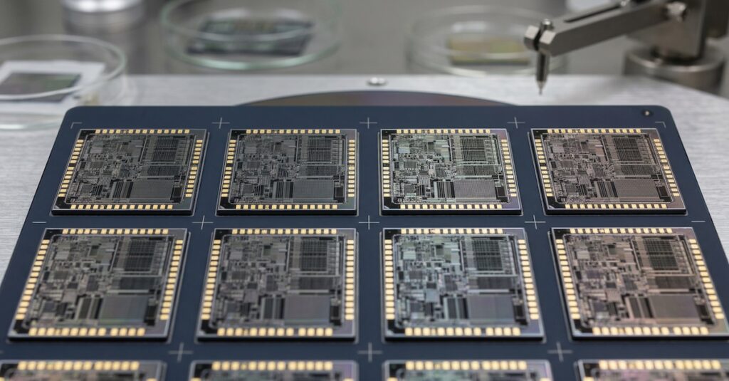
Image Generated Using DALL·E
The semiconductor industry is at a turning point. For decades, progress followed a well-defined path: scale transistors, shrink nodes, and watch performance and efficiency improve.
However, as I discussed in The Role of Simulation in Semiconductor Product Development, this formula alone is no longer sufficient. Physical and economic barriers are making each new node more expensive, more complex, and slower to deliver.
In this environment, innovation cannot rely solely on lithography advances, it has to come from how we design, validate, and manufacture chips.
This is where digital twins are emerging as a critical enabler. Unlike static simulations, digital twins are dynamic, data-driven models that replicate the behavior of physical components, equipment, and processes in real-time.
They represent not just a tool, but a new way of thinking about product development, one that connects design, manufacturing, and reliability into a continuous loop of learning and improvement.
Why Digital Twins
At their core, digital twins aim to bridge the gap between the physical and the virtual. They allow engineers to build a living, breathing model of a chip, a process, or even an entire fab, one that evolves with real-time data and can be tested under countless scenarios. Unlike traditional simulations, which are static and limited to a specific design phase, digital twins continuously adapt, creating a feedback loop between design, manufacturing, and reliability.
As I explored in The Semiconductor Smart Factory Basics, smart factories already rely on sensors and analytics to monitor performance and drive efficiency. Digital twins extend this idea further by enabling the virtual modeling of entire systems, optimizing recipes, validating workflows, and reducing risks before they reach the production floor. The value extends beyond the fab.
In The Semiconductor Reliability Testing Essentials, I discussed how AI-driven modeling can anticipate failures long before physical tests are complete. Digital twins take this predictive approach to the next level, embedding reliability into the earliest stages of design and ensuring that potential weaknesses are addressed before chips even leave the drawing board.
By reducing costly iterations, lowering the reliance on physical prototypes, and enabling continuous learning across the product lifecycle, digital twins are becoming not just a competitive advantage but a necessity in the post-Moore era.
Digital Twins In Action
The promise of digital twins becomes clear when we examine how they transform specific stages of semiconductor product development, design, reliability, and manufacturing.
Smarter Design Cycles: Instead of relying on lengthy trial-and-error processes with physical prototypes, digital twins enable the validation of architectures and exploration of design trade-offs virtually. In The Role of Simulation in Semiconductor Product Development, I discussed how simulation already reduces risks and accelerates iteration. Digital twins extend this idea by creating dynamic models that update with real-world data, ensuring that the “virtual chip” always reflects the current state of development.
Predictive Reliability: Reliability is one of the most expensive and time-consuming parts of the semiconductor lifecycle. As noted in The Semiconductor Reliability Testing Essentials, AI-driven prediction can reduce reliance on long burn-in tests. Digital twins add another layer by modeling how devices behave under stress, heat, or aging, allowing engineers to simulate years of use in hours. This helps identify weak points early and deliver more robust products.
Yield and Process Optimization: Yield is the ultimate measure of success in manufacturing. In Data-Driven Approaches to Yield Prediction in Semiconductor Manufacturing, I highlighted how analytics can drive better yield outcomes. Digital twins take it a step further by simulating entire fab processes, testing different recipes, and identifying bottlenecks without risking live wafers. This leads directly to higher throughput, less scrap, and more predictable manufacturing outcomes.
Continuous Learning: The most transformative aspect of digital twins is how they turn every stage of development into a feedback loop. Each test, each process tweak, and each reliability check feeds back into the virtual model, making it smarter over time.
Bottlenecks To Overcome
For all their promise, digital twins in semiconductors face significant hurdles. As I noted in The Semiconductor Data-Driven Decision Shift, traditional EDA tools were never designed for system-level interactions across chiplets, packaging, and fab processes.
Scaling digital twins requires integrating data from design simulations, equipment sensors, and reliability testing into one unified model, a challenge compounded by siloed workflows and the sheer volume of data modern fabs generate. Without seamless interoperability, the value of the twin remains limited.
Economic and practical constraints add another layer of complexity. Building high-fidelity digital models, validating them across various operating conditions, and maintaining their accuracy in real-time is a resource-intensive process.
As noted in The Economics of Semiconductor Yield, profitability often hinges on razor-thin margins. For digital twins to scale, the industry must establish standards, reduce the costs of adoption, and prove clear ROI. Until then, many companies will hesitate to embrace this transformative approach despite its long-term potential fully.
Ultimately the companies that master digital twins will not only reduce risks and accelerate product cycles but also redefine what progress looks like in the post-Moore era. Just as chiplets and AI are reshaping architectures, digital twins are reshaping development itself.