RECENT BLOG Post
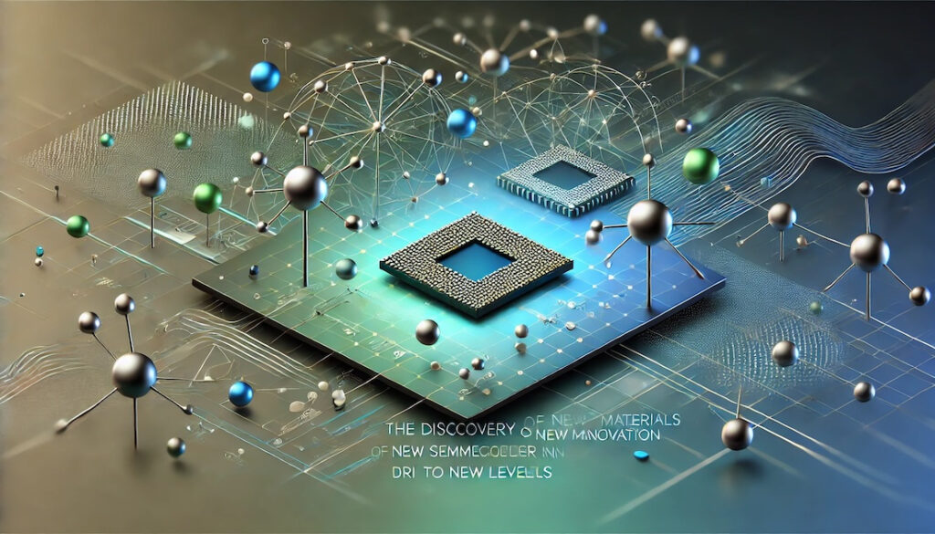
DALL-E Why New Materials Are Needed The semiconductor industry has been built on the backbone of silicon for decades.
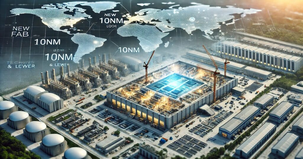
DALL-E The Surge In Fab Construction It is no secret that the semiconductor industry is seeing an unprecedented boom
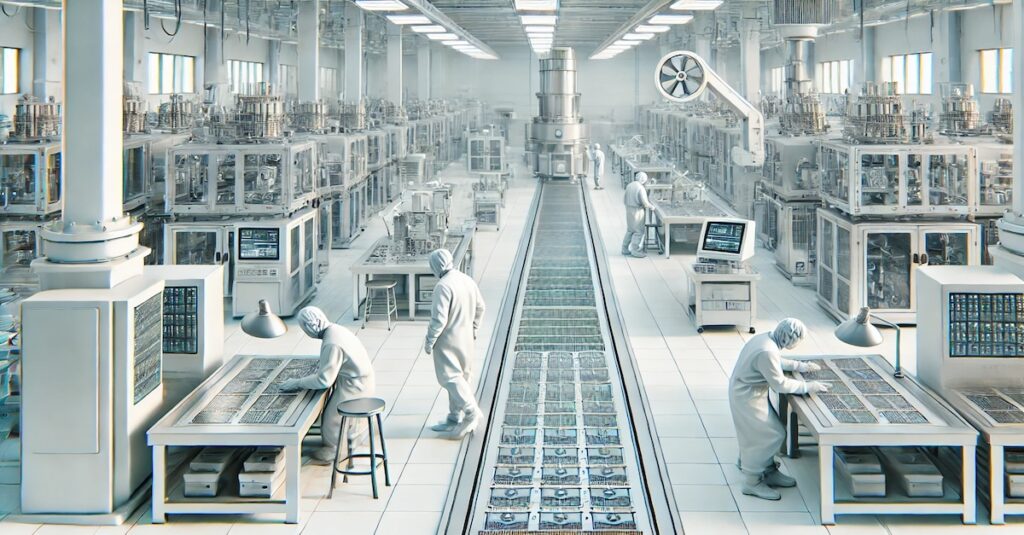
DALL-E FAB And Yield Yield in semiconductor manufacturing is a complex concept that measures the efficiency and effectiveness of
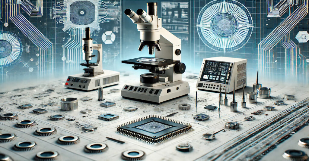
DALL-E Precision And Semiconductors Precision is not just a technical term in semiconductor manufacturing. It is the foundation on
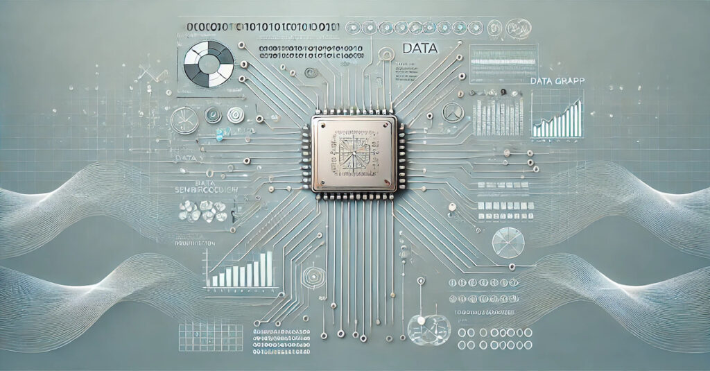
DALL-E Understanding LLM And AI Agents LLM-based models like GPT have been developed to comprehend, create, and interact with
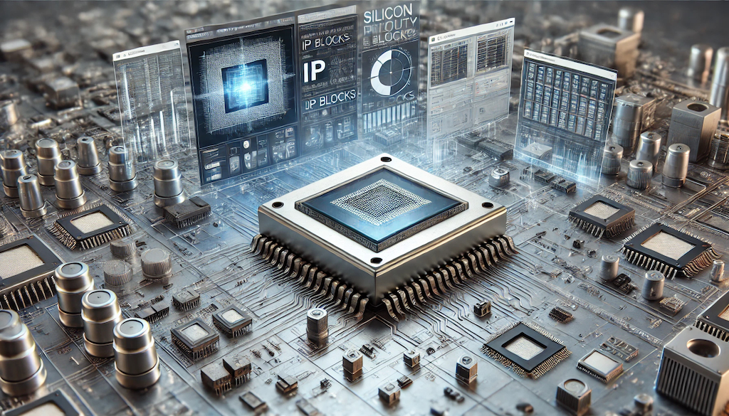
DALL-E The Importance Of IP In Semiconductors Semiconductors are powering everything from smartphones to advanced AI systems. The IP
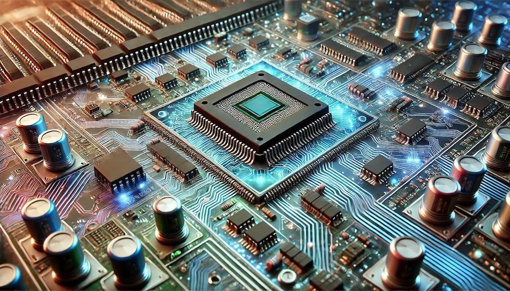
DALL-E Semiconductors And PCB Semiconductors play a crucial role in modern electronic devices by providing processing, memory, and logic

DALL-E The Dual Imperative Of Innovation And Sustainability In Semiconductor Manufacturing Semiconductors are the backbone of countless technologies, from
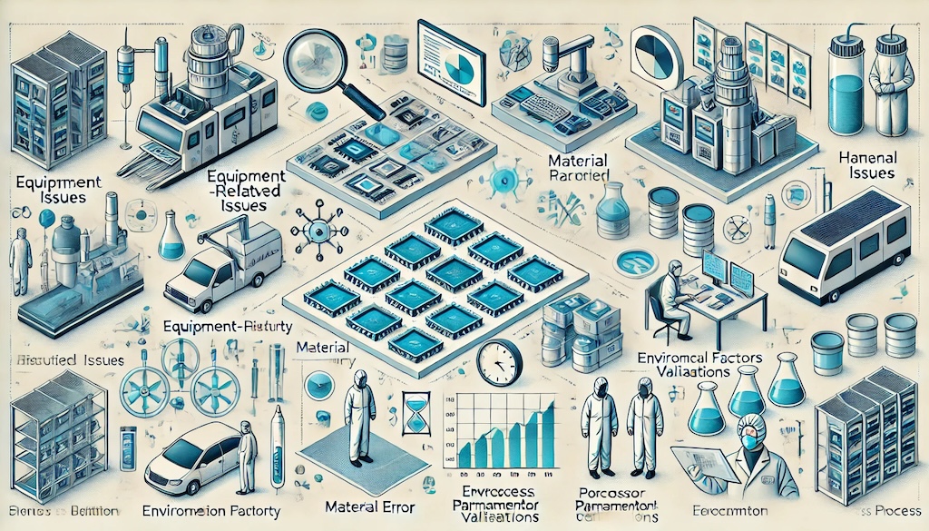
DALL-E Yield, Cost Efficiency And Product Quality Understanding the various types of semiconductor yield is essential for optimizing production