Image Generated With GPT Image 2.0
Compute Scaling Alone Is No Longer Enough
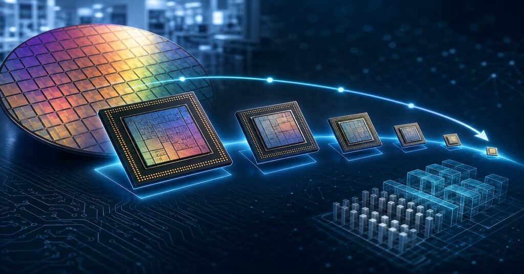
For decades, semiconductor progress was driven primarily by transistor scaling. Smaller transistors enabled higher compute density, faster performance, and lower power consumption, allowing continuous system level improvements across multiple generations of computing infrastructure.
Today, that scaling model is changing.
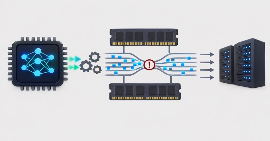
Modern Artificial Intelligence (AI) systems are increasingly constrained not only by compute capability, but by how efficiently data moves between compute engines, memory, accelerators, and distributed infrastructure. Training and inference workloads require enormous bandwidth across highly parallel architectures, making communication efficiency critical to sustaining performance.
This challenge is becoming more visible as accelerator performance scales faster than memory bandwidth and interconnect capability. Modern Graphics Processing Units (GPUs) and AI accelerators can process massive workloads internally, but maintaining utilization requires moving enormous amounts of data across increasingly complex system architectures.
Power consumption further amplifies the problem. In many advanced systems, transporting data across interconnects, substrates, and board level channels consumes more energy than the compute operations themselves. As communication distances increase, latency, signal integrity, thermal density, and power efficiency become increasingly difficult to manage.
As a result, the semiconductor industry is shifting focus from transistor scaling alone toward communication efficiency optimization. Bandwidth density, latency reduction, energy per bit, and memory proximity are now becoming central architectural priorities across modern compute infrastructure.
Advanced Packaging Has Become A Communication Technology
Advanced packaging has also emerged as one of the most important technologies enabling modern data movement scaling. Traditional monolithic System on Chip (SoC) architectures are increasingly limited by reticle size constraints, escalating advanced node costs, and yield challenges associated with very large die sizes.
To address these limitations, the industry is rapidly transitioning toward heterogeneous integration and chiplet based architectures. Instead of integrating all functionality onto a single monolithic die, modern systems partition compute, memory, Input/Output (I/O), analog, and accelerator functions across multiple specialized dies assembled within a single package.
This transition fundamentally changes the role of packaging.
| Technology | Primary Communication Role | Key Benefit | Primary Challenge |
|---|---|---|---|
| Monolithic SoC | On die communication | Lowest latency | Reticle and yield limits |
| 2.5D Interposer | High density die connectivity | Massive bandwidth scaling | Cost and complexity |
| HBM Integration | Memory proximity | Extremely high memory bandwidth | Thermal constraints |
| Advanced Organic Substrates | Package routing scalability | Lower cost integration | Routing density limitations |
| Embedded Bridge Architectures | Localized die interconnect | Efficient bandwidth scaling | Assembly complexity |
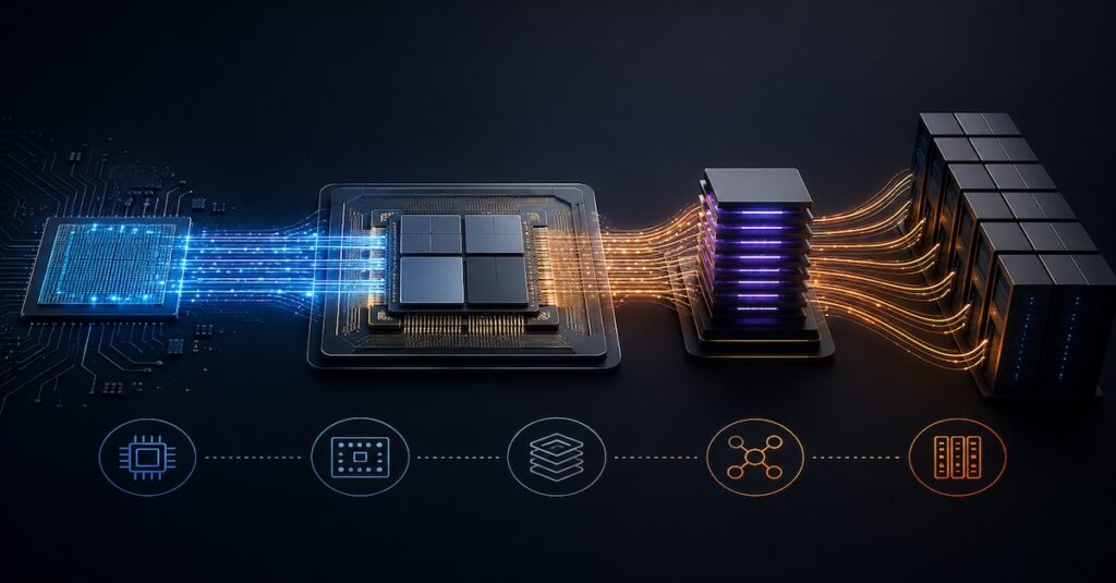
Packaging is no longer simply a mechanical integration layer. It has become the primary communication fabric that determines how efficiently data moves within modern semiconductor systems. Technologies such as 2.5D silicon interposers, advanced organic substrates, fan out redistribution layers, and embedded bridge architectures now provide ultra high density die to die interconnect capability that was previously achievable only within monolithic silicon.
High Bandwidth Memory (HBM) integration represents one of the clearest examples of this shift. AI accelerators increasingly rely on tightly integrated HBM stacks positioned adjacent to compute dies using silicon interposers or advanced substrate technologies. This physical proximity enables thousands of parallel interconnects operating simultaneously, dramatically improving memory bandwidth while reducing communication latency and power consumption.
The package itself is increasingly becoming the system level optimization boundary. Partitioning decisions are now influenced heavily by communication efficiency, thermal management, power delivery, and manufacturability considerations. As architectures become more disaggregated, advanced packaging increasingly determines overall system capability.
Scale Out Infrastructure Is Expanding The Data Movement Problem
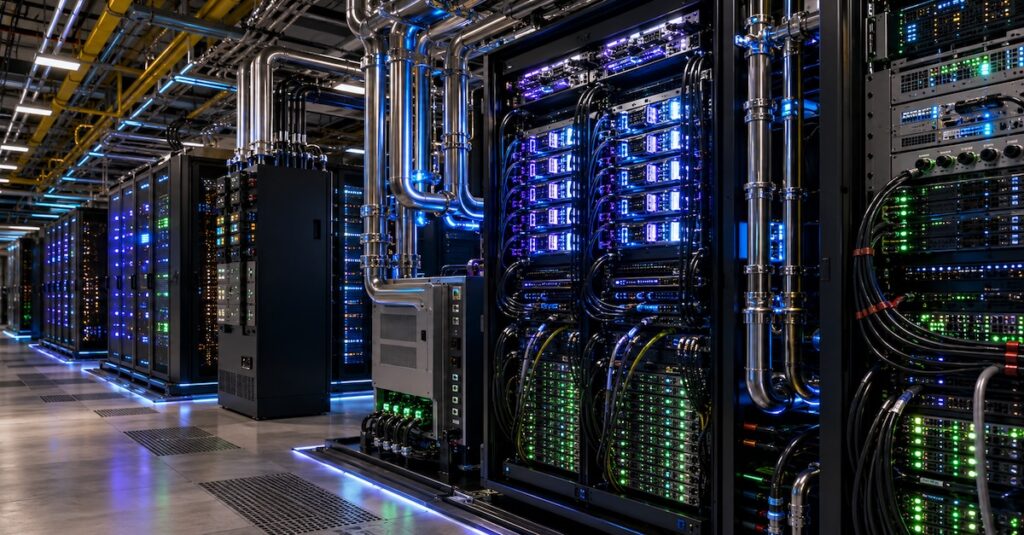
While advanced packaging improves communication efficiency within a package, modern AI infrastructure increasingly depends on large scale distributed systems that extend across servers, racks, and entire data centers. Training advanced AI models now requires thousands of accelerators operating simultaneously across highly interconnected clusters, making efficient data movement between systems critical to overall performance.
As these architectures scale outward, electrical communication becomes increasingly difficult to sustain. Longer electrical traces introduce signal degradation, higher power consumption, insertion loss, thermal complexity, and growing latency challenges. Maintaining signal integrity at extremely high bandwidths across rack scale distances is becoming one of the major infrastructure bottlenecks for AI systems.
To address these limitations, the industry is moving toward new connectivity architectures such as Co Packaged Optics (CPO) and Co Packaged Copper (CPC). By integrating communication technologies closer to switching silicon and accelerators, these approaches reduce electrical path lengths while improving bandwidth scalability and power efficiency.
This transition reflects a broader industry shift toward distributed communication centric computing. Modern AI infrastructure increasingly operates as interconnected compute fabrics where communication efficiency between accelerators directly impacts throughput, scalability, and overall system utilization.
Communication Efficiency Will Define Future Semiconductor Scaling
The growing importance of data movement is reshaping semiconductor design priorities. Historically, performance scaling focused primarily on compute density and transistor efficiency. Today, communication efficiency across compute, memory, package, and infrastructure domains is becoming equally critical.
Architecture teams now optimize systems around memory proximity, bandwidth hierarchy, interconnect topology, and power efficient communication. At the same time, advanced packaging and multi die integration are increasing manufacturing and test complexity, requiring tighter assembly tolerances and more sophisticated package level validation.
The role of test is also expanding throughout the semiconductor lifecycle. Multi die systems require validation not only of individual dies, but also of die to die interconnect reliability and high speed communication behavior under real workloads.
The semiconductor industry is no longer scaling through transistor density alone. The next phase of innovation will increasingly depend on how efficiently data can move across increasingly disaggregated systems.