Image Generated With GPT Image 2.0
State Of Silicon Agents
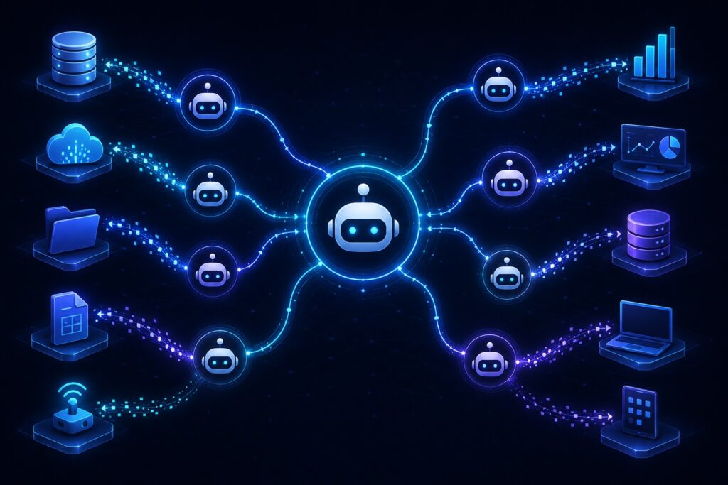
Artificial intelligence in semiconductors is rapidly moving beyond copilots and analytics dashboards. The industry is now entering the era of semiconductor agents, where AI systems can autonomously analyze data, optimize workflows, coordinate engineering tasks, and increasingly make operational decisions across design, manufacturing, packaging, and test.
Unlike traditional automation, semiconductor agents operate with contextual awareness. They interact across multiple software environments, consume large engineering datasets, and execute iterative tasks with limited human intervention. This transition is becoming necessary because semiconductor complexity is scaling faster than engineering capacity.
Modern AI accelerators now involve thousands of interconnected design components, advanced packaging structures, heterogeneous chiplets, and increasingly constrained manufacturing flows. The scale of data generation across Electronic Design Automation (EDA), fab operations, test, yield analytics, and supply chain systems is becoming impossible to manage manually alone.
From AI Assistance To Agentic Semiconductor Workflows
The strongest signal that semiconductor agents are becoming real comes from the EDA ecosystem.
Synopsys introduced its “AgentEngineer” strategy focused on AI driven semiconductor design workflows capable of handling increasingly autonomous engineering tasks. According to Reuters, the company is building AI agents that can execute specific chip design activities such as verification and testing while eventually coordinating large multi chip system development.
This matters because semiconductor design complexity is no longer centered around a single monolithic die. AI infrastructure systems now involve hundreds or thousands of interconnected chips, advanced packaging topologies, memory stacks, and system level optimization constraints. Traditional engineering workflows are struggling to scale with this complexity.
Synopsys also outlined a longer term roadmap toward increasingly autonomous engineering operations, including AI copilots for Register Transfer Level (RTL) generation, verification assistance, timing analysis, and design debugging.
Similarly, Cadence Design Systems has expanded AI assisted design workflows using machine learning based optimization platforms. Cadence and TSMC jointly demonstrated AI driven Design Rule Check (DRC) optimization that improved debugging efficiency during advanced node development.
These are early forms of semiconductor agents. Today they assist engineers. Tomorrow they will orchestrate large portions of the workflow autonomously.
Semiconductor Manufacturing Is Becoming Agent Driven
The foundry and manufacturing side of the industry is also evolving toward agentic operations.
TSMC has increasingly discussed AI enabled manufacturing optimization involving yield improvement, defect analysis, process monitoring, and fab orchestration. Industry analysis shows that AI systems are already being used to improve production learning cycles, optimize yield, and coordinate complex manufacturing operations.
Agentic manufacturing systems are increasingly being applied in several areas:
| Manufacturing Area | Emerging Agent Function |
|---|---|
| Yield Engineering | Autonomous defect correlation and yield learning |
| Lithography Optimization | Process parameter tuning and overlay optimization |
| Test Operations | Adaptive test flows and dynamic screening |
| Equipment Maintenance | Predictive failure analysis |
| Supply Chain Coordination | Dynamic material and capacity allocation |
| Advanced Packaging | Assembly optimization and thermal reliability analysis |
This shift is becoming increasingly critical as advanced semiconductor manufacturing generates massive volumes of process data across lithography, deposition, etch, metrology, inspection, assembly, and test operations. At advanced nodes, the scale, speed, and multidimensional complexity of these datasets have surpassed the limits of traditional human driven analysis.
Semiconductor organizations are now turning toward AI driven agents and autonomous analytics systems to accelerate yield learning, identify process excursions faster, optimize manufacturing decisions in real time, and improve overall operational efficiency across increasingly complex manufacturing environments.


