Image Generated Using Nano Banana
Two Worlds Of AI Compute Are Finally Colliding
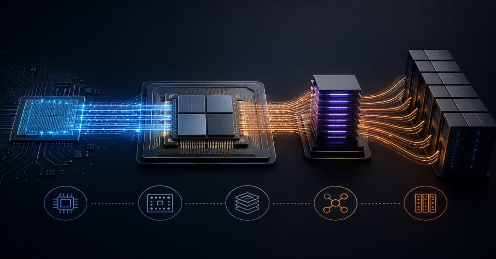
For more than a decade, AI silicon has evolved along two independent trajectories. On one side sat throughput-optimized architectures built to train massive models across thousands of accelerators. These prioritize raw FLOPS, memory bandwidth, and scaling efficiency. On the other hand, latency-optimized designs were engineered to deliver fast, deterministic inference. They are used at the edge or in tightly constrained data center environments. Each solved a different bottleneck, served a different buyer, and spoke a different architectural language.
That division made sense when training and inference occurred separately. Training was infrequent and centralized in hyperscale data centers. Inference ran continuously, near users, under strict latency and power limits. Chip companies specialized: some in large-scale matrix math, others in microsecond responsiveness, real-time scheduling, and efficient small-batch execution.
The AI boom of the last few years has collapsed that neat divide. Large language models, multimodal systems, and agentic AI now blur the boundary between training and inference. Models are fine-tuned continuously and updated frequently. They are increasingly deployed in interactive settings. Here, response time directly shapes user experience. In this environment, solving only for throughput or only for latency is no longer sufficient.
As a result, a structural shift is underway in the semiconductor industry. Chip companies that historically dominated one side of the equation are responding. They are acquiring, partnering, or redesigning their architectures to address the other side. When latency-first and throughput-first philosophies converge under a single entity, the impact extends far beyond product roadmaps. This shift reshapes how AI computing is designed, deployed, and monetized across the entire ecosystem.
Latency Versus Throughput And Economic Tradeoffs
Latency-optimized and throughput-optimized chips differ in almost every major design choice, reflecting different workload, integration, and cost assumptions.
Latency-focused architectures emphasize minimizing response time for individual requests by optimizing for small batch sizes, predictable execution paths, and efficient handling of workloads with extensive control logic. These chips commonly serve inference for recommendation systems, conversational AI, and autonomous systems.
In contrast, throughput-focused architectures maximize processing of large, regular workloads through aggressive parallelism, making them suited for the prolonged training of massive neural networks.
The table below summarizes key architectural distinctions:
| Dimension | Latency-Optimized Architectures | Throughput-Optimized Architectures |
|---|---|---|
| Primary Goal | Minimize response time | Maximize total compute per unit time |
| Typical Workload | Inference, real-time AI | Training, large-scale batch jobs |
| Batch Size | Small to single-request | Large, highly parallel batches |
| Memory Behavior | Low latency access, caching | High bandwidth, streaming |
| Interconnect | Limited or localized | High-speed, scale-out fabrics |
| Power Profile | Efficiency at low utilization | Efficiency at high utilization |
| Software Stack | Tight HW-SW co-design | Framework-driven optimization |
As a result, this convergence exposes inefficiencies when architectures stay siloed. Throughput-optimized chips can struggle to deliver consistent, low-latency inference unless you overprovision. Latency-optimized chips often lack the scaling efficiency needed for large-scale model training. The economic consequence is fragmented infrastructure and a rising total cost of ownership.
What Happens When One Company Owns Both Sides Of The Equation
When a single chip company unites the industry’s best latency and throughput solutions, the impact transcends simple product expansion. This move redefines design philosophy, software stacks, and customer value propositions.
From an architecture standpoint, convergence enables more balanced designs. Unified companies can deliberately trade off between peak throughput and tail latency, rather than blindly optimizing for a single metric. We are already seeing accelerators that support flexible batching, adaptive precision, and mixed workloads, allowing the same silicon platform to serve training, fine-tuning, and inference with fewer compromises.
Software is where the impact becomes most visible. Historically, separate hardware platforms required separate toolchains, compilers, and optimization strategies. Under one entity, these layers can be harmonized. A single software stack that understands both training and inference enables smoother model transitions from development to deployment, reducing friction for customers and shortening time-to-value.
The table below highlights how unified ownership changes system-level outcomes:
| Aspect | Fragmented Latency / Throughput Vendors | Unified Architecture Vendor |
|---|---|---|
| Hardware Portfolio | Specialized, siloed products | Co-designed, complementary products |
| Software Stack | Multiple toolchains | Unified compiler and runtime |
| Customer Workflow | Disjoint training and inference | Seamless model lifecycle |
| Infrastructure Utilization | Overprovisioned, inefficient | Higher utilization, shared resources |
| Innovation Pace | Incremental within silos | Cross-domain optimization |
| Strategic Control | Dependent on partners | End-to-end platform leverage |
Strategically, this convergence decisively strengthens negotiating power with both hyperscalers and enterprise customers. Vendors delivering a coherent training-to-inference platform command stronger positions in long-term contracts and ecosystem partnerships.
Consequently, there is also a competitive implication. Unified vendors can shape standards and influence frameworks. They can guide developer behavior in ways fragmented players cannot. As AI computing shifts from a commodity to a strategic asset, control over both latency and throughput becomes industrial power.
New Center Of Gravity In AI Compute
The convergence of latency and throughput architectures marks a turning point for the AI semiconductor industry. A technical distinction is now a strategic divide. Some companies offer isolated solutions. Others provide integrated platforms.
As training and inference workloads merge, chip companies treating AI compute as a continuous lifecycle will win. This approach avoids viewing each step as a separate phase. Combining latency and throughput optimized solutions brings architectural balance. It enables software coherence and economic efficiency.
This shift marks a new center of gravity for the AI ecosystem, as compute is no longer just about speed or scale. Now, it is about adaptability and utilization.
It also supports changing AI needs without frequent infrastructure redesign.