Image Generated Using DALL·E
The Layered AI Stack And The Semiconductor Roots
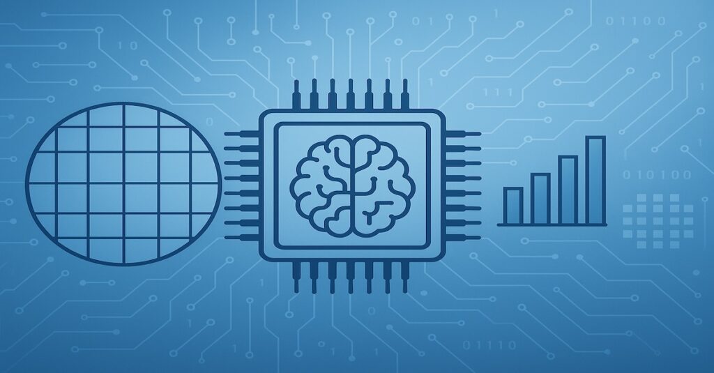
Artificial intelligence operates through a hierarchy of interdependent layers, each transforming data into decisions. From the underlying silicon to the visible applications, every tier depends on semiconductor capability to function efficiently and scale economically.
The AI stack can be imagined as a living structure built on four essential layers: silicon, system, software, and service.
Each layer has its own responsibilities but remains fundamentally connected to the performance and evolution of the chips that power it. Together, these layers convert raw computational potential into intelligent outcomes.
At the foundation lies the silicon layer, where transistor innovation determines how many computations can be executed per joule of energy. Modern nodes, such as those at 5 nm and 3 nm, make it possible to create dense logic blocks, high-speed caches, and finely tuned interconnects that form the core of AI compute power.
| AI Stack Layer | Example Technologies | Semiconductor Dependence |
|---|---|---|
| Silicon | Logic, memory, interconnects | Determines compute density, power efficiency, and speed |
| System | Boards, servers, accelerators | Defines communication bandwidth, cooling, and energy distribution |
| Software | Frameworks, compilers, drivers | Converts algorithmic intent into hardware-efficient execution |
| Service | Cloud platforms, edge inference, APIs | Scales models to users with predictable latency and cost |
Above this, the system layer integrates the silicon into servers, data centers, and embedded platforms. Thermal design, packaging methods, and signal integrity influence whether the theoretical performance of a chip can be achieved in real-world operation.
Once silicon is shaped into functional systems, software becomes the crucial bridge between mathematical models and physical hardware. Frameworks such as TensorFlow and PyTorch rely on compilers like XLA and Triton to organize operations efficiently across GPUs, CPUs, or dedicated accelerators. When these compilers are tuned to the architecture of a given chip, its cache size, tensor core structure, or memory hierarchy, the resulting improvements in throughput can reach 30-50 percent.
At the top of the stack, the service layer turns computation into practical value. Cloud APIs, edge inference platforms, and on-device AI engines rely on lower layers to deliver low-latency responses at a global scale. Even a modest reduction in chip power consumption, around ten percent, can translate into millions of dollars in savings each year when replicated across thousands of servers.
In essence, the AI stack is a continuum that begins with electrons moving through transistors and ends with intelligent experiences delivered to users. Every layer builds upon the one below it, transforming semiconductor progress into the computational intelligence that defines modern technology.

AI Value From Transistors To Training Efficiency
The value of artificial intelligence is now measured as much in terms of energy and computational efficiency as in accuracy or scale. Every improvement in transistor design directly translates into faster model training, higher throughput, and lower cost per operation. As process nodes shrink, the same watt of power can perform exponentially more computations, reshaping the economics of AI infrastructure.
Modern supercomputers combine advanced semiconductors with optimized system design to deliver performance that was previously unimaginable.
The table below illustrates how leading AI deployments in 2025 integrate these semiconductor gains, showing the connection between chip architecture, energy efficiency, and total compute output.
| AI Supercomputer / Project | Company / Owner | Chip Type | Process Node | Chip Quantity | Peak Compute (FLOP/s) |
|---|---|---|---|---|---|
| OpenAI / Microsoft – Mt Pleasant Phase 2 | OpenAI / Microsoft | NVIDIA GB200 | 5 nm | 700 000 | 5.0 × 10¹⁵ |
| xAI Colossus 2 – Memphis Phase 2 | xAI | NVIDIA GB200 | 5 nm | 330 000 | 5.0 × 10¹⁵ |
| Meta Prometheus – New Albany | Meta AI | NVIDIA GB200 | 5 nm | 300 000 | 5.0 × 10¹⁵ |
| Fluidstack France Gigawatt Campus | Fluidstack | NVIDIA GB200 | 5 nm | 500 000 | 5.0 × 10¹⁵ |
| Reliance Industries Supercomputer | Reliance Industries | NVIDIA GB200 | 5 nm | 450 000 | 5.0 × 10¹⁵ |
| OpenAI Stargate – Oracle OCI Cluster | Oracle / OpenAI | NVIDIA GB300 | 3 nm | 200 001 | 1.5 × 10¹⁶ |
| OpenAI / Microsoft – Atlanta | OpenAI / Microsoft | NVIDIA B200 | 4 nm | 300 000 | 9.0 × 10¹⁵ |
| Google TPU v7 Ironwood Cluster | Google DeepMind / Google Cloud | Google TPU v7 | 4 nm | 250 000 | 2.3 × 10¹⁵ |
| Project Rainier – AWS | Amazon AWS | Amazon Trainium 2 | 7 nm | 400 000 | 6.7 × 10¹⁴ |
From these figures, it becomes clear that transistor scaling and system integration jointly determine the value of AI. Each new semiconductor generation improves energy efficiency by roughly forty percent, yet the total efficiency of a supercomputer depends on how well chips, networks, and cooling systems are co-optimized.
The GB300 and B200 clusters, built on advanced 3nm and 4nm processes, deliver near-exponential performance per watt compared to earlier architectures. Meanwhile, devices such as Amazon Trainium 2, based on a mature 7nm node, sustain cost-effective inference across massive cloud deployments.
Together, these systems illustrate that the future of artificial intelligence will be shaped as much by the progress of semiconductors as by breakthroughs in algorithms. From mature 7 nm inference chips to advanced 3 nm training processors, every generation of silicon adds new layers of efficiency, capability, and intelligence.
As transistors continue to shrink and architectures grow more specialized, AI value will increasingly be defined by how effectively hardware and design converge. In that sense, the story of AI is ultimately the story of the silicon that powers it.