The Case For Energy-Aware Semiconductor Lithography
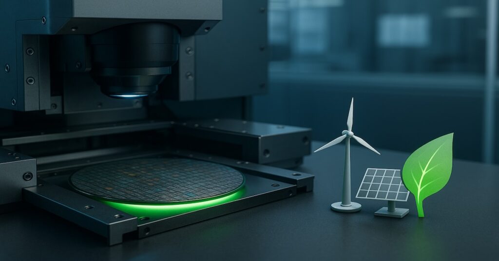
DALL·E Rising Energy Burden Of Lithography Lithography has become one of the most energy-intensive stages in the fabrication of wafers. As fabs push to 2 nm and below, every additional patterning layer increases electricity demand and associated CO₂ emissions. Industry projections now indicate that wafer-fab emissions will exceed approximately 270 Mt CO₂e by 2030, primarily from equipment-driven loads. Fabs cannot treat lithography power as a fixed cost anymore. High-NA EUV, expected to be widely deployed in high-volume environments, delivers the resolution needed for advanced logic. However, it also increases per-tool power requirements, precisely the kind of “performance/energy ↑” tradeoff that sustainability teams are trying to mitigate. This imbalance is the reason lithography is now being singled out in sustainability roadmaps. What “Energy-Aware” Really Means Energy-aware lithography integrates […]
The Case For Energy-Aware Semiconductor Lithography Read More »