Image Generated Using Nano Banana
AI Is Becoming Essential In Semiconductor Manufacturing
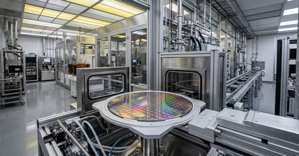
Semiconductor manufacturing is an intricate, highly specialized process involving hundreds to thousands of tightly controlled steps, where even slight variations impact yield and performance.
For decades, engineers and technicians used statistical process control and expertise to maintain process stability. Now, modern fabs generate terabytes of data daily from sensors, inspection tools, and test systems, overwhelming traditional analytics tools.
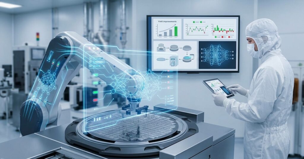
This shift lets Artificial Intelligence and machine learning play a vital role in semiconductor manufacturing. AI delivers actionable insights across thousands of process variables, optimizing yields, reducing scrap, cutting downtime, and streamlining production. Early failure identification boosts efficiency and enables faster, data-driven decisions.
AI and machine learning are now rapidly transforming semiconductor manufacturing.
Traditional Manufacturing Vs AI-Driven Manufacturing
The shift toward AI in semiconductor manufacturing becomes clearer when we directly compare traditional engineering approaches with AI-driven methods.
For decades, semiconductor fabs relied on statistical process control, rule-based inspection systems, and manual engineering analysis to monitor production. These approaches were effective when manufacturing data volumes were smaller and process complexity was more manageable.
| Traditional Semiconductor Manufacturing | AI-Driven Semiconductor Manufacturing |
|---|---|
| Relies heavily on manual engineering analysis and statistical process control | Uses machine learning models to analyze thousands of process variables simultaneously |
| Root cause analysis often occurs after yield loss or defect detection | Predictive analytics identifies potential process deviations before defects occur |
| Equipment maintenance is scheduled or reactive | Predictive maintenance forecasts tool failures using sensor data |
| Inspection relies on rule-based algorithms and pixel comparison | AI vision systems identify complex defect signatures and adapt to new defect patterns |
| Process optimization cycles may take weeks or months | AI accelerates process optimization and reduces problem-resolution time |
Building on this comparison, in traditional fabs, engineers often analyze process data after a yield excursion has already occurred. In contrast, AI systems shift this paradigm toward predictive manufacturing, where early process signatures indicate potential downstream issues before they become costly failures.
Furthermore, AI sharply reduces yield loss. Studies show that AI-driven defect detection and optimization can cut yield loss, directly boosting efficiency and slashing costs.
Real World Implementations
AI in semiconductor manufacturing has moved beyond theory. Industry leaders now use AI for defect detection, yield analytics, predictive maintenance, and process optimization in actual production environments.
The following examples show how major players integrate AI into real manufacturing workflows.
| Organization | AI Application | Description |
|---|---|---|
| Micron Technology | AI-Driven Image Analytics | Micron uses AI-based image analytics to analyze inspection images across manufacturing stages, helping engineers detect anomalies and improve yield and quality. |
| Lam Research | Digital Twin and AI Yield Optimization | Lam Research developed Fabtex Yield Optimizer, which uses machine learning and digital-twin models to analyze fab data and improve process performance in high-volume manufacturing. |
| TSMC | AI-Driven Smart Manufacturing | TSMC has deployed AI techniques to improve equipment maintenance, optimize yield learning, and enable smart manufacturing within advanced fabs. |
| Intel | AI-Enhanced Process Control | Intel applies machine learning to analyze lithography and process data, enabling faster root-cause detection and improved process control across fabs. |
| Samsung Electronics | AI-Based Defect Detection | Samsung uses AI vision systems to improve wafer inspection and defect classification, enabling more accurate defect identification and process monitoring. |
These examples demonstrate that AI adoption in semiconductor manufacturing is already well underway. Rather than replacing engineering expertise, AI is increasingly serving as a decision-support layer, enabling engineers to interpret large manufacturing datasets more effectively. As fabs continue to generate massive volumes of process and inspection data, AI tools will likely become an integral component of future semiconductor manufacturing infrastructure.
Toward Intelligent Semiconductor Factories
Initially, AI faced skepticism in semiconductor manufacturing due to the complex nature of fab operations and the need for precise process control. The explosion of manufacturing data and the increased complexity of technology nodes have since driven AI adoption.
Today, AI systems enable earlier defect detection, predictive equipment maintenance, faster yield optimization, and improved process control across manufacturing environments.
Within the semiconductor manufacturing ecosystem, AI increasingly serves as a decision-support layer, helping engineers navigate massive datasets, uncover hidden correlations, and make faster, more informed decisions. Rather than replacing engineering expertise, AI strengthens it by enabling deeper insights into process behavior and manufacturing variability.
As AI becomes embedded across design, manufacturing, and testing stages of chip production, the debate is no longer about whether AI belongs in semiconductor manufacturing.
Instead, the focus is shifting toward how far the industry can advance toward intelligent, autonomous fabs and how quickly those possibilities can become reality.